1.55 Micron Emission from InAs/InP Self-Assembled Quantum Dots
- PDF / 1,586,049 Bytes
- 6 Pages / 417.6 x 639 pts Page_size
- 77 Downloads / 344 Views
ABSTRACT Self-assembled InAs/InP and InAs/InGaAsP quantum dots (QDs) grown by metal-organic chemical vapour epitaxy (MOVPE) exhibit emission at 1.5-1.6 gm at room temperature. P-I-N diodes incorporating a single InAs/InGaAsP QD layer exhibit strong electroluminescence over a wide range of input currents and emit significantly more light per layer than a InGaAs/InGaAsP multi-quantum well device.
INTRODUCTION Self-assembled QDs are the subject of intense study since they promise ultra-low threshold, temperature independent lasers with high differential gains which are eminently suitable for short haul low power optoelectronic devices [1,2]. InAs/GaAs is the most intensely investigated system with devices operating around 1gm [3], although recent developments have led to photodiodes and LEDs operating at 1.3gm [4,5]. It is arguable that the formation, size, shape and composition of QDs in this system is determined by the segregation effects of indium. There has been much less work on other Ill-V combinations where the formation of QDs also occurs. This paper presents results obtained for the InAs/InP and InAs/InGaAsP systems which demonstrate room temperature photoluminescence (PL) and electroluminescence (EL) around 1.55gim. In this case the formation of QDs is attributed to As/P exchange since In is common throughout the structure. The realisation of QD lasers in this long wavelength region would be an important development since Auger recombination, which is highly temperature sensitive, represents the major loss mechanism in 1.55gm devices and should be suppressed in a QD structure.
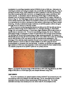
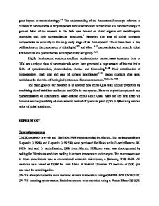
EXPERIMENTAL PROCEDURE The samples investigated here were grown by MOVPE using trimethylgallium, arsine and phosphine as source gases. The substrate temperature was kept as low as possible whilst still ensuring good surface morphology. A disadvantage of MOVPE compared with molecular beam epitaxy is the lack of an in situ monitoring method such as RHEED which indicates when the 2D-3D transition has occurred. Thus the approach adopted here is more empirical although the results are repeatable. Sulfur doped (001) InP substrates (cut 0.35' towards (110)) were used throughout. Except for the p-i-n diodes the structures consisted of an undoped InP buffer layer grown at 650TC at a growth rate of 1.2 gmh-'. The temperature was either maintained at 650TC or reduced to 600TC for growth of an InP (type A) or InGaAsP quaternary (Q) (type B) layer at a growth rate of 0.14 gmh1. The InAs layers (1-4 monolayers (ML) thick) were also deposited at a low growth rate at temperatures in the range 500-600 0 C. Growth interrupts were not used in 159 Mat. Res. Soc. Symp. Proc. Vol. 571 c 2000 Materials Research Society
this work. The structures were then capped by 0.01tm InP or Q at the low growth rate followed by 0.04tnm of cap material at the faster growth rate. Some samples were grown without cap layers for Atomic Force Microscopy (AFM) or Scanning Electron Microscopy (SEM) measurements. The p-i-n structures were similar to those described above using
Data Loading...