A microstructural investigation of the bcc to A15 phase transition in sputter-deposited Nb 3 Al superconductors
- PDF / 3,051,109 Bytes
- 6 Pages / 612 x 792 pts (letter) Page_size
- 66 Downloads / 230 Views
ANGand S, D. DAHLGRENare Senior Research Scientist, Metallurgy Research Section, and Manager, Surface Science Section, respectively, Materials Department, Battelle Northwest, RicMand,Washington 99352. Manuscript submitted April t 1, 1977. METALLURGICALTRANSACTIONSA
EXPERIMENTAL
PROCEDURES
A Nb3AI deposit (0,I mm thick) was prepared by a dc triode, high-rate sputter-deposition technique, 4 The substrate was a 3.8 cm diameter polished copper disc and it was water cooled to nearly 10~ The deposition was made from a compacted powder target of niobium and aluminum using 1500 eV krypton. A deposition rate of 1 pm/min was achieved. The deposit was r e moved from the substrate by dissolving the copper substrate in nitric acid, and then it was cut into 3 mm diameter disc microscopy samples with an electron discharge machine. Samples were encapsulated in quartz tubes at 133.3 x 10"~ P a and heat treated at 500, 550, 600, 650 and 700~ for 24 h. Thin foils for TEM studies were prepared by jet thinning of the m i c r o scopy samples using 5 parts HF, 5 parts HNO3 and 10 parts H20 a t - 20~ RESULTS The resutts showed there were four distinct m i c r o structural stages associated with the bcc-to-A15 phase transition of the sputter-deposited and heat treated Nb3A1: 1) The bcc-NbsA1 deposit at 10~ 2) the segregation of the bcc-Nb3A1 solid solution (500 to 600~ 3) the nucleation and growth of the A15 phase (650~ and 4) the A15 phase (700~ bcc-NbsA1 Deposited at t0~ The m i c r o s t r u c t u r e of the NbsAt deposited at 10~ shows a fine-grained bcc phase containing many defeCtSo(Fig, l(a)). The average grain size is nearly 1000A with grains ranging from 500 to 5000,~. A defect structure of dislocation networks and fine precipitates was observed in the grains (Fig. l(b)). The defect structure of the bcc-Nb3A1 resembled the m i c r o structure of as-deposited Cu-0.15 wt pct Zr made by high-rate sputter deposition, 8 which showed high-density dislocations pinned by fine precipitates. This type VOLUME 8A, NOVEMBER 1977-1763
(a)
(c)
(b)
(d)
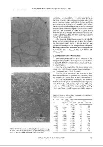
Fig. 1--Microstructure and electron diffraction patterns from bcc-Nb3A1 as-sputter-deposited at 10~ (a) Electron micrograph of the fine grained microstructure, (b) electron micrograph showing the defect structure of fine precipitates and dislocation networks, (c) diffraction pattern showing only a single bcc phase, (d) diffraction pattern of a single grain showing only a single bec phase.
Segregation of the bcc-Nb3Al Solid Solution (500 to 600~C) of as-deposited m i c r o s t r u c t u r e is characteristic of the high-rate, sputter-deposited solid solutions of compositions that are beyond the equilibrium solid solubility limits. Only the single bcc phase is indicated by the electron diffraction patterns in Figs. l(c) and (d); the precipitates were evidently not large enough to be detected in the diffraction pattern.
1764-VOLUME 8A, NOVEMBERt977
No notable grain growth of bcc-Nb3A1 was found for heat treatments at 500~ and 550~ for 24 h; however, the dislocation density was reduced and th
Data Loading...


