A Phase Diagram for Morphology and Properties of Low Temperature Deposited Polycrystalline Silicon Grown by Hot-wire Che
- PDF / 1,616,874 Bytes
- 6 Pages / 612 x 792 pts (letter) Page_size
- 68 Downloads / 255 Views
A8.11.1
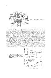
A Phase Diagram for Morphology and Properties of Low Temperature Deposited Polycrystalline Silicon Grown by Hot-wire Chemical Vapor Deposition Christine E. Richardson, Maribeth S. Mason and Harry A. Atwater, Thomas J. Watson Laboratory of Applied Physics, California Institute of Technology, Pasadena, CA 91125, U.S.A ABSTRACT The fabrication of low temperature polycrystalline silicon with lifetimes close to single crystalline silicon, but with internal surface passivation similar to that observed in deposited microcrystalline silicon, is a promising direction for thin film polycrystalline silicon photovoltaics. To achieve this, large grains with passivated grain boundaries and intragranular defects are required. We investigate the low-temperature (250-550ºC) epitaxial growth of thin silicon films by hot-wire chemical vapor deposition (HWCVD) on Si(100) substrates and large-grained polycrystalline silicon template layers formed by selective nucleation and solid phase epitaxy (SNSPE). Using reflection high energy electron diffraction (RHEED) and transmission electron microscopy (TEM), we have observed epitaxial, twinned epitaxial, mixed epitaxial/polycrystalline and polycrystalline phases in the 50 nm–15 µm thickness regime. HWCVD growth on Si(100) was performed using a mixture of diluted silane (4% in He) and hydrogen at a H2/SiH4 ratio of 50:1 at substrate temperatures from 300–475ºC. We will discuss the relationship between the microstructure and photoconductive decay lifetimes of these undoped layers on Si(100) and SNSPE templates as well as their suitability for use in thin-film photovoltaic applications. INTRODUCTION HWCVD epitaxial growth on large-grained templates is one strategy for the fast low-temperature growth of large-grained films with hydrogen-passivated low-angle grain boundaries. We propose a structure by which a template with 100 micron diameter grains is fabricated on ITO-coated glass by a solid-phase crystallization process called SNSPE [1]. This layer will serve as the n+ layer, and the p and p+ layers would be grown epitaxially on this template by HWCVD, using tri-methyl boron as a dopant. Preliminary work towards the fabrication of this cell is discussed. EXPERIMENTAL DETAILS In order to promote crystalline growth, we used a high hydrogen partial pressure dilution ratio of 50:1, using a mixture of 4% SiH4 in He at a partial pressure of 25 mTorr and 50 mTorr H2. The half millimeter diameter tungsten wire was positioned 2.5 cm from the substrate for a growth rate of 1Å/s. The wire temperature was set to 1800ºC as measured by optical pyrometry, and substrate temperatures ranged from 300ºC to 475ºC. Silicon (100) and large-grained polycrystalline layers formed by SNSPE were used as templates for epitaxial growth. The formation of the large-grained templates is described elsewhere [1]. The resulting polycrystalline templates have grain sizes on the
A8.11.2
order of 100 µm with low-angle grain boundaries. Before growth, surfaces were cleaned with UV ozone for 10 minutes followed by an HF d
Data Loading...