a-SiN:H Thin Film Diode for Digital Radiography
- PDF / 361,523 Bytes
- 5 Pages / 612 x 792 pts (letter) Page_size
- 3 Downloads / 301 Views
a-SiN:H THIN FILM DIODE FOR DIGITAL RADIOGRAPHY I.A. POPOV, G. VAN DOORSELAER, A. VAN CALSTER, H. DE SMET, J. DE BAETS*, F. CALLENS, E. BOESMAN** *
ELIS-TFCG/IMEC, University of Ghent, Ghent, Belgium CSSS, University of Ghent, Ghent, Belgium
**
ABSTRACT Recent developments in the area of cost effective 2D direct x-ray sensor arrays on the base of a-SiN:H back-to-back Schottky diodes and no switching devices per pixel are presented. Discussion focuses on two major aspects: (i) x-ray sensitivity of the sensor itself and possibility of its improvement; (ii) the overall performance of the sensor array. INTRODUCTION
Number of photons
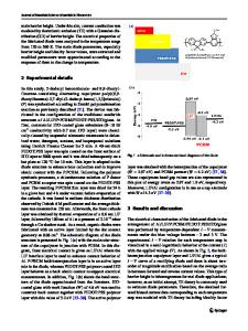
Digital radiography for medical and industrial purposes attracts a lot of attention for a long time already. Substitution of screen/film systems with digital ones has a lot of advantages, including environmental – such as silverless technology and exclusion of photo film development steps - and productivity – such as increased throughput. Currently there is a variety of systems under development that use a-Si:H alloys. The widest application of a-Si:H alloys in the digital radiography is information retrieval from pixels. As a rule the systems use active matrix of a-Si:H thin-film transistors (AM TFT) for pixel control. In some applications, where x-ray radiation is converted before registration, a-Si:H alloys find use as a sensors – a-Si:H photo diodes in [1] or a-Si:H Schottky diodes in [2]. Limited to the information retrieval part, a-Si:H alloys devices have never been used for direct x-ray sensing due to low weight of the atoms and low density of the structural network. From this point of view a-Si:H alloys are weak contestants to a-Se [3] or PbO [4]. Nevertheless, there seems to be a niche for the use of a-Si:H alloys for both information acquisition and retrieval. If realised this will lead to cost-effective, high yield, low voltage 2D x-ray sensor arrays, with no need to combine dif1 ferent technologies in one process. 0.9 Figure 1 shows typical distribution of 0.8 o photons by energies from the 17 W anode tube 0.7 at 80 kV (3 mm Al filter). As it can be seen from 0.6 the data, the most of generated photons have an 0.5 energy in the range 30 - 50 keV - mean photon 0.4 energy is 47 keV. After travelling the distance of 0.75 m the original spectrum is modified due to 0.3 absorption by air and the average photon energy 0.2 drops even further - to 37.7 keV. This data illus0.1 trates the fact that in x-ray radiography with en0 ergies below 100 keV the major part of informa0 10 20 30 40 50 60 70 tion is delivered by photons with energies at Energy, keV around 40 keV. In fact, one may focus on reFigure 1. 80 keV 17o W anode energy trieving information from low energy photons spectrum. (many photons, low penetration efficiency) ac-
A12.9.1
cepting that information delivered by high energy photons (fewer photons, high penetration efficiency) will not be used efficiently. This draws a natural limit on detectable maximum energy of incoming x-ray radiation. Targeting detection of photons
Data Loading...