Ab Initio Modeling of Contact Structure Formation of Carbon Nanotubes and Its Effect on Electron Transport
- PDF / 991,727 Bytes
- 6 Pages / 612 x 792 pts (letter) Page_size
- 79 Downloads / 482 Views
1081-P07-25
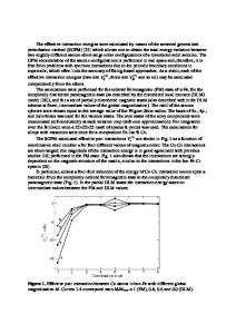
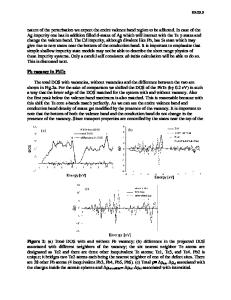
Ab Initio Modeling of Contact Structure Formation of Carbon Nanotubes and Its Effect on Electron Transport Weiqi Luo1, Karthik Ravichandran1, Wolfgang Windl1, and Leonardo R.C. Fonseca2 1 The Ohio State University, Columbus, OH, 43210 2 Universidade Estadual de Campinas, Campinas, 13083-870, Brazil ABSTRACT Carbon nanotube (CNT) devices are studied as a possible alternative to the current silicon based CMOS technology. The contacts between CNTs and metal electrodes in such devices exert great influence on the device performance. In this study, ab initio temperature accelerated dynamics are performed to study the contact formation between CNTs and Ti electrodes. Results indicate that CNTs undergo significant structural deformation, resulting in a significant decrease of the device conductance. This finding may explain the discrepancy between experimental and simulated results in molecular devices. However, more effects may need to be taken into account as we discuss for the example of the size effect of CNTs. INTRODUCTION The minimization of silicon based devices has been an effective approach to speed up the integrated circuits (ICs) and to fabricate more transistors into a chip for more than three decades. However, it is well known that this continuous development is not sustainable for much longer without modifying the device underlying configurations and employing new materials because the feature size of current ICs is approach several physical limits. One of the possible alternatives are molecular electronics. These are defined as electronics whose properties are determined by the chemical, physical, and electronic structures of molecules. This definition is very broad; it includes conductive polymers and even the insulating polymer layers on metal wiring. In common use, molecular electronics refers to molecular structures whose characteristic features are on the nanoscale containing between one and a few thousand molecules. Remarkable progress in this field has been made in the last few years, as researchers have developed ways of growing, addressing, imaging, manipulating, and measuring small groups of molecules connecting metal leads. Several prototype devices such as conducting wires, insulating linkages, rectifiers, switches, and transistors have been demonstrated[1]. In parallel, there has been significant theoretical activity toward developing the description of nonequilibrium transport through molecules[2]. It is hard to say whether in time such devices could conceivably complement the current silicon-based integrated circuit (IC) industry or generate entirely new areas of applicability. It is clear, however, that in any case models will have to be developed to describe large-bias transport through ultrasmall devices, whether based on silicon or molecules. The fundamental challenge for modeling molecular electronics involves determining the structure/property relationships for electronic transport (intra- or intermolecular) through a junction containing one or a few molecules as the transpo
Data Loading...