Ab Initio Structure Characterization for the Amorphous Assembly of Si Clusters Encapsulating Transition Metal
- PDF / 316,415 Bytes
- 6 Pages / 432 x 648 pts Page_size
- 11 Downloads / 320 Views
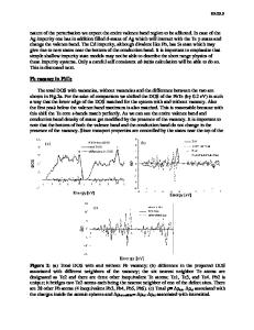
Ab Initio Structure Characterization for the Amorphous Assembly of Si Clusters Encapsulating Transition Metal Takehide Miyazaki1, Noriyuki Uchida2, and Toshihiko Kanayama3 1 Nanosystem Research Institute, National Institute for Advanced Industrial Science and Technology, 1-1-1 Umezono, Tsukuba, Ibaraki 305-8568, Japan 2 Nanoelectronics Research Institute, National Institute for Advanced Industrial Science and Technology, 1-1-1 Higashi, Tsukuba, Ibaraki 305-8562, Japan 3 National Institute for Advanced Industrial Science and Technology, 1-1-1 Umezono, Tsukuba, Ibaraki 305-8568, Japan ABSTRACT We present a first-principles lattice dynamics for the assembly of the transition-metal (M)-encapsulated Sin clusters in amorphous phase (a-MSin), which has been proposed as a potential candidate for the channel material of the next-generation thin-film transistors (TFTs) [N. Uchida et al., Appl. Phys. Express 1, 121502 (2008)]. The shape of calculated vibrational density of states (VDOS) curve of a-MoSi10 is similar to the counterpart of the high pressure phase of aSi (HPA-Si) although the present systems are obtained as a result of pressure relaxation. Its radial distribution function (RDF) among Si themselves is characterized by the absence of a gap between the first and second shells, which is also the case in . We further present the VDOS of aWSi10, whose curve shape is again similar to that of HPA-Si. A difference between a-MoSi10 and a-WSi10 is that the W-atom displacement components extracted from the vibration eigenvectors are mainly distributed over a lower frequency range (< ~ 150 cm-1) than the Mo counterpart (~ 150 cm-1 to ~ 300 cm-1). This may be attributed to a larger atomic mass of W than Mo. INTRODUCTION While hydrogenated amorphous Si (a-Si:H) has been a principal material for thin-film transistors (TFTs), it suffers from degradation of its electrical properties due to the StaeblerWronsky effect (SWE) [1]. A widely accepted remedy for this drawback is to replace a-Si:H by micro-crystalline Si (P-Si). However, aggressive downsizing of the TFTs with P-Si might be difficult since grains in P-Si may induce the spatial fluctuation of the channel properties on the nano-meter scale. In order to achieve both the SWE-free nature and the atomic scale granularity, fabrication of yet another class of Si-related materials is necessary. Recently, novel amorphous semiconductors (a-MSin, M=Mo or Nb, 7 ≤ n ≤ 16) with relatively high carrier mobilities have been synthesized [2]. The materials were grown by the deposition of M-encapsulating Si clusters. The Hall measurement showed the p- and n-type semiconducting characters of a-MoSin and a-NbSin, respectively. The Raman shift spectra of aMoSi12 and a-NbSi13 suggested that a-Si-like network occurs without H. Thus the materials were assumed to be stabilized as the assembly of the deposited clusters, where the M atoms terminated the Si dangling bonds (DBs) and hence suppress the electronic disorder. The above insight was supported by ab initio structure optimization of a-MoSi12
30
Data Loading...