Adhesion of Crystalline GeSbTe/TiN Interface Characterized by Four Point Bend, Nanoindentation, and Nanoscratch
- PDF / 265,264 Bytes
- 6 Pages / 612 x 792 pts (letter) Page_size
- 5 Downloads / 279 Views
0997-I10-09
Adhesion of Crystalline GeSbTe/TiN Interface Characterized by Four Point Bend, Nanoindentation, and Nanoscratch Guohua Wei1, Jun Liu2, David Fillmore1, Mike Violette2, and Shifeng Lu1 1 Surface Analysis Laboratory, Micron Technology, Boise, ID, 83707 2 R & D Department, Micron Technology, Boise, ID, 83707
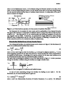
ABSTRACT Reversible structural phase change phenomenon of certain chalcogenide materials has been investigated extensively in the past decades. Among various phase change chalcogenide materials, Ge2Sb2Te5 (GST) is the most studied material due to its superior optical, electrical and mechanical properties. One of the challenges in using GST is the poor adhesion between crystalline GeSbTe (c-GST) and the substrate, such as TiN. In this work, the adhesion of the cGST/TiN interface of two samples deposited by different techniques was characterized using four-point bend, nanoindentation and nanoscratch techniques. The nanoindentation and nanoscratch data agree well with the four point bend data. The paper also discusses the application potential of nanoindentation and nanoscratch techniques as qualitative methods for adhesion evaluation in semiconductor process development. INTRODUCTION Chalcogenide phase change materials exhibit many interesting optical and electrical properties such as large reversible variation of optical reflectivity and electrical resistivity between their amorphous and crystalline states [1]. These unique optical and electrical properties of chalcogenide phase change materials lead to various practical applications. Among the variety of chalcogenide phase change materials that have been investigated in the past, Ge2Sb2Te5 (GST) is the most commonly utilized material due to its superior optical, electrical and mechanical properties [2, 3]. However, poor adhesion between GST and the surrounding materials could lead to data loss or hard failure after prolonged device cycling or undesirable process issues [4]. With regards to the concern of GST interfacial adhesion, we developed various deposition techniques to improve the GST interfacial adhesion and applied different characterization techniques to evaluate the GST adhesion to substrate. This paper studies the adhesion of GST/TiN interfaces, which were deposited differently, by four point bend [5], nanoindentation [6-8] and nanoscratch [9-11] techniques. EXPERIMENT The blanket thin film samples studied in this work were: 150nm c-GST/100nm TiN/240 nm TEOS/Si. Two sets of samples, Sample A and B were prepared with different deposition techniques. Sample A was DC-sputtered, and sample B was RF-sputtered.
The adhesion of Sample A and B were studied using four-point bend, nanoindentation and nanoscratch techniques. The four-point bend tests were conducted on a DTS Delaminator (Menlo Park, CA) following the procedures described in [5]. Nanoindentation and nanoscratch tests were performed using a MTS Nano Indenter XP system (Oak Ridge, TN), equipped with the Dynamic Contact Module (DCM) and nanoscratch options. The DCM option was used to do
Data Loading...