AlN Wafers Fabricated by Hydride Vapor Phase Epitaxy
- PDF / 1,029,058 Bytes
- 5 Pages / 612 x 792 pts (letter) Page_size
- 47 Downloads / 363 Views
ABSTRACT We report on AlN wafers fabricated by hydride vapor phase epitaxy (HVPE). AlN thick layers were grown on Si substrates by HVPE. Growth rate was up to 60 microns per hour. After the growth of AlN layers, initial substrates were removed resulting in free-standing AlN wafers. The maximum thickness of AlN layer was about 1 mm. AlN free-standing single crystal wafers with a thickness ranging from 0.05 to 0.8 mm were studied by x-ray diffraction, transmission electron microscopy, optical absorption, and cathodoluminescence.
INTRODUCTION AlN substrates are needed for high-power microwave devices based on group III nitride heterostructures and UV photodetectors. High-performance GaN-based microwave transistors and solar-blind photodetectors have already been demonstrated on sapphire and SiC substrates. AlN substrates are expected to improve device characteristics further due to close lattice- and thermal-match with GaN-based device structures, high thermal conductivity and good insulating properties. High quality AlN materials have been grown in thin layer form, but bulk growth of AlN is much more difficult technological task. Main methods to grow bulk AlN are sublimation [1] and growth from a melt [2]. Experimental AlN crystals of about 15 mm in diameter have been reported for laboratory development [3]; commercial AlN wafers are not available. Recently, we have demonstrated high quality AlN materials grown by the HVPE method [4]. AlN layers about 0.5 µm thick were grown on 6H-SiC substrates. Cathodoluminescence of AlN was measured at room temperature revealing edge peak at photon energy of 5.9 eV. The minimum value of the full width at a half maximum (FWHM) of ω-scan x-ray rocking curve was about 120 arc sec. The value of the specific resistivity of AlN was found to be 1013 Ohm cm at 300 K and 108 Ohm cm at 700 K. In this paper, we report on HVPE growth of thick (up to 1 mm) AlN layers.
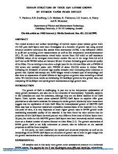
EXPERIMENTAL PROCEDURE AND RESULTS AlN deposition experiments were carried out on the HVPE growth machine equipped with horizontal open-flow hot wall reactor and two-zone resistively heated furnace (Fig. 1). One zone is the source zone and another is the growth zone. The maximum growth zone temperature is 1200 oC. Substrate temperature for AlN was varied
F99W6.5 Downloaded from https://www.cambridge.org/core. IP address: 146.185.200.99, on 15 Apr 2019 at 21:21:17, subject to the Cambridge Core terms of use, available at https://www.cambridge.org/core/terms. https://doi.org/10.1557/S1092578300004609
from 900oC to 1200oC. In our HVPE processes, Ar serves as a carrier gas. Ammonia and HCl are supplied from gas tanks. A boat containing metallic Al was placed in Al source tube. Substrates were placed on quarts pedestal in the growth zone of the reactor. AlN layers were grown using a reaction between aluminum chloride and ammonia. Aluminum chloride gas was formed by reaction between metallic Al and HCl, and was transported from the source zone to the growth zone by Ar flow.
Ar growth zone
source zone NH 3+Ar
substrate
HCl+Ar
Data Loading...