Aluminum Thermo Compression Bonding Characterization
- PDF / 275,387 Bytes
- 6 Pages / 612 x 792 pts (letter) Page_size
- 78 Downloads / 321 Views
1222-DD04-02
Aluminum Thermo Compression Bonding Characterization
E. Cakmak1, V. Dragoi2, E. Pabo1, T. Matthias1, and T. Alford3 1 EV Group Inc., 7700 S. River Parkway, Tempe, AZ 85284, USA 2 EV Group, DI E. Thallner 1, 4782-St. Florian/Inn, AUSTRIA 3 School of Materials, Arizona State University, Tempe, AZ, 85287 USA
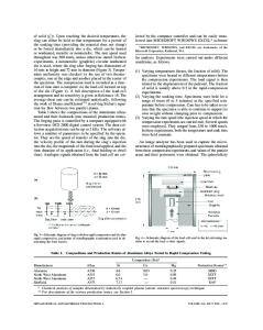
ABSTRACT Wafer level bonding is an important technology for the manufacturing of numerous microelectromechanical systems. In this work the aluminum thermo-compression wafer bonding is characterized. The effects and significance of various bond process parameters and surface treatment methods are reported on the final bond interfaces integrity and strength. Experimental variables include the bonding temperature, bonding time, and bonding atmosphere (forming gas and inert gas). Bonded wafer samples were investigated with scanning acoustic microscopy, scanning electron microscopy, and four point bending test. Interfacial adhesion energy and bond quality were found to be positively correlated with bonding temperature. A bonding temperature of 500 ºC or greater is necessary to obtain bond strengths of 8-10 J/m2. INTRODUCTION Wafer bonding processes are used in Microelectromechanical Systems (MEMS) manufacturing because they allow the construction of three dimensional structures and wafer level packaging. The different wafer level bonding processes such as silicon (Si) direct, anodic, glass frit, polymer, metal thermo-compression (TCB) and eutectic all have specific requirements and performance. The application, use, requirements, and wafer bonding process conditions differ significantly with the application type [1]. Metal TCB is one of the techniques used for MEMS fabrication as it enables a high degree of hermeticity, electrical interconnect and minimum area consumption by the bond line. Physical, chemical, electrical, and thermodynamic properties of the given material play a crucial role in the feasibility of the bonding process and must be considered during the design stage of an application. The choice of aluminum (Al) is based on the fact it has been used for decades in chip manufacturing as the main metallization material. The compatibility with Complementary–Metal–Oxide–Semiconductor (CMOS) technology and existing infrastructure recommends Al TCB as a promising technology in CMOS-MEMS integration. The TCB of two metal surfaces of the same material is a solid state reaction and relies on the inter-diffusion of atoms and grain growth along the bond interface [2]. This bond is created by the application of high force to the wafer stack under high temperatures for extended periods of time. By increasing the temperature the material hardness decreases which therefore reduces the amount of pressure necessary to bring the two surfaces into immediate contact. Diffusion rates are a function of temperature; therefore increased temperature yields higher diffusion rates. The interface grain growth is greatly inhibited by metal oxides on the initial surfaces. Ideally the
metal surface is oxide-free prior to
Data Loading...