An in Situ STM Study of Cu and Ni Electrodeposition
- PDF / 4,442,357 Bytes
- 6 Pages / 414.72 x 648 pts Page_size
- 90 Downloads / 333 Views
Mat. Res. Soc. Symp. Proc. Vol. 404 01996 Materials Research Society
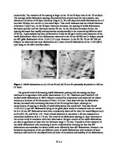
investigation of nickel deposition was performed using a concentrated electrolyte of 1.5 mol/l Ni(S0 3NH 2)2 (Fluka), 0.5 mol/l H 3BO3 with a pH of 3.5. RESULTS AND DISCUSSION SubstratePreparationand StructuralCharacterization- Immediately prior to multilayer deposition, the Cu substrates were typically immersed in 10 mmol/l HCl for 5-30 minutes. The solution was open to the atmosphere (i.e. oxygen) which results in etching of the surface [4, 5] and the formation of large (100) terraces on the miscut Cu(100). For short pretreatment times this results in a RMS surface roughness on the order of - 1.4 nm over a 100 jim 2 area. The terraces are completely covered by a ('12 x 412)R450 Cl adlattice as determined by LEED and in situ STM [6, 7, 8]. As shown in Fig. 2, a high resolution constant current STM image obtained at -0.25 V vs. Cu/Cu+ reveals a series of terraces bounded by oriented steps. The step orientation is in sharp contrast to the close packed orientation associated with clean copper surfaces in UHV systems [9]. The step edge corresponds to the close packed direction of the chlorine adlattice. Similar observations of the influence of a ('12 x 42)R450 oxygen adlayer on the step structure of Ni(100) in vacuum were recently reported [10]. In the present case, the chloride adlattice has a dominant influence on the binding energy of an adatom to a step as well the activation energy for migration along a step edge and thereby controls the evolution of the step morphology on Cu(100). Interestingly, the importance of enhanced step edge mobility relative to terrace mobility has been previously noted for Cu atoms on clean Cu(100) in UHV[11]. This results in kink saturated metal steps beneath the adlattice. The monoatomic step height Cu top layer -0.18 nm corresponds to copper (ao = 0.361). ,'"
. i0
Cs 10101
Cu bottom layer
ca [oool
Fig. 1. A 13 x 13 nm STM image of (12 x 12)R45o chlorine adlattice on Cu(100) at -0.169 V vs. Cu/Cu+ in 10 mmol/l HCl with Etip = 0.120 V, it--9.0 nA, and a frame time of 32 s. A schematic of the proposed chlorine adlayer structure is also shown. In contrast to halide media, immersion in 10 mmol/l sulfuric or perchloric acid results in an ill-defined surface step structure and obtaining reliable atomically resolved images of Cu(100) proved difficult. The importance of halide adsorption on the electrochemical processing of copper is highlighted by its ubiquitous presence as an additive in most commercial copper electroplating baths [12]. Reductive Desorptionof Chlorine Adlattice - The oxidatively adsorbed adlayer of chlorine may be reduced to chloride at negative potentials as shown by LEED and AES studies [6]. The voltammetric signature associated with this process on Cu(1 11) was recently reported [13]. Desorption occurs at potentials more positive than that associated with heteroepitaxial nickel deposition and the structural ramifications of this reaction are of some importance to the growth of multilayered material
Data Loading...