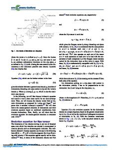
Analysis of Dislocation Behavior in Low Dislocation Density, PVT-Grown, Four-Inch Silicon Carbide Single Crystals
- PDF / 23,233,150 Bytes
- 6 Pages / 612 x 792 pts (letter) Page_size
- 89 Downloads / 386 Views
1246-B02-02
Analysis of Dislocation Behavior in Low Dislocation Density, PVT-Grown, Four-Inch Silicon Carbide Single Crystals M. Dudley,1 S. Byrappa,1 H. Wang,1 F. Wu,1 Y. Zhang,1 B. Raghothamachar,1 G. Choi,1 E. K. Sanchez,2 D. Hansen,2 R. Drachev,2 and M.J. Loboda2 1 Department of Materials Science and Engineering, Stony Brook University, Stony Brook, NY, USA 11794-2275 2 Dow Corning Compound Semiconductor Solutions, Midland, Michigan, USA 48686-0994 ABSTRACT Synchrotron White Beam X-ray Topography studies are presented of dislocation behavior and interactions in a new generation of one hundred millimeter diameter, 4H-SiC wafers grown using Physical Vapor Transport (PVT) under specially designed low stress conditions. Such low stress growth conditions have, for example enabled reductions of basal plane dislocation (BPD) densities by two or three orders of magnitude compared to previous levels down to just a few hundred per square centimeter. This provides a unique opportunity to discern details of dislocation behavior which were previously precluded due to complications of image overlap at higher densities. Among the phenomena observed in these studies is the deflection of threading dislocations onto the basal plane producing various stacking fault configurations. Analysis of the contrast from these faults enables determination of their fault vectors which, in turn, provides insight into their possible formation mechanisms. INTRODUCTION The detrimental influence of defects such as dislocations on SiC device performance [1-4] has made the lowering of their densities a primary goal of the SiC crystal growth community. Synchrotron White Beam X-ray Topography (SWBXT) has, over the past two decades, played a key role in revealing the detailed configurations of these defects and has been able to shed much light on their origins [5,6] thereby supporting the development of strategies for their elimination. Included among the notable contributions are the identification of threading screw dislocations (TSDs) and threading edge dislocations (TEDs) as growth defects [7-9] and BPDs as deformation induced defects [5]. The latter has promoted the development of stress reduction strategies to minimize the driving force for BPD motion behind the growth interface. In a previous paper [10], we reported the reduction of thermal shear stress during growth to levels below the critical resolved shear stress of 1 MPa which enabled the lowering of BPD densities by up to three orders of magnitude in both 76 and 100mm wafers. This provided a unique opportunity to discern details of BPD behavior which were previously mostly irresolvable such as the repeated deflection of threading edge dislocations onto the basal plane followed by redirection into threading orientation. In this paper, we present further results of SWBXT studies carried out on similar wafers cut (with 4° offcut towards [1120] ) including observations of the deflection of other types of threading dislocations onto the basal plane which produce various kinds of stacking fault