Analysis of Strain in GaN on Al 2 O 3 and 6H-SiC: Near-Bandedge Phenomena
- PDF / 426,226 Bytes
- 6 Pages / 414.72 x 648 pts Page_size
- 111 Downloads / 235 Views
Mat. Res. Soc. Symp. Proc. Vol. 395 0 1996 Materials Research Society
8
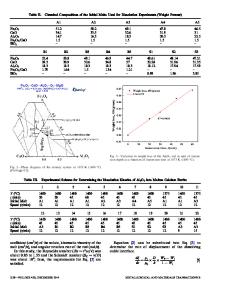
Fig. 1. Pseudodielectric function of a 1.32 gim thick GaN film on a 6HSiC substrate. These data are approximated by a model calculation where < of a consists F2> broadened unit step edge followed by a linear ramp.
6 A V 2
3
2
E (eV)
7 meV
A V
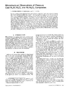
Fig. 2. Imaginary part of the pseudodielectric function of GaN layers grown on A12 0 3 (upper) and 6H-SiC (lower). The spectra were taken with a resolution of 2 meV.
2A
18 meV
V
0
'-7 3.40
3.35
3.45
3.50
E (eV)
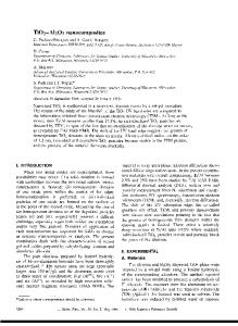
E Fig. 3. Calculated variation of the A, B, and C absorption thresholds relative to the top of the valence band as a function of crystal-field and biaxial stress potentials. A spin-orbit splitting of 15.5 meV was used. -10
VcF+V•(meV)
406
p that is actually measured by ellipsometry was converted into a pseudo or apparent dielectric function = + i by means of the two-phase (substrate/ambient) model. The spectrum of Fig. 1, which was obtained on a 1.32 micron thick GaN film deposited on 6H-SiC, exhibits characteristic interference oscillations in the region of transparency below the fundamental absorption edge at 3.4 eV, relatively sharp structure in both and at the edge, and a nearly linearly increasing behavior in above the edge. Also shown in Fig. 1 is an approximate analytic representation of the lineshape that will be described below. Figure 2 provides a more detailed view of the variation of with energy in the vicinity of the absorption edge for two samples, a 3.27 pm thick GaN layer grown on A12 0 3 (upper) and a 1.45 prm thick GaN layer grown on SiC (lower). Here, the fine structure due to the A and B thresholds is evident, with splittings of about 7 and 18 meV, respectively, in the two cases. We consider first the implications of the A-B splittings shown in Fig. 2. The energy variations of the A, B, and C thresholds can be described in the quasicubic model [7] in terms of 3 parameters: the spin-orbit splitting energy Vso, the crystal-field potential Vcf, and the rhombohedral strain parameter V,. The dependence of these threshold energies on these three parameters have been given by Pollak and Cardona [8]. In essence, in the quasicubic model the effect of hexagonal symmetry is described as a deformation of the cube along the [111] direction. Thus for uniform biaxial strain in the plane of the film Vd and V,, are additive, and the results can be expressed in terms of the sum of these two terms. These observations open up the possibility of band structure engineering through the intentional variation of in-plane strain. Calculated variations of the energies of the A, B, and C thresholds with respect to the top of the unperturbed valence band of the equivalent cubic material are shown as a function of the sum (Vcf + V.) in Fig. 3, along with the A-B splitting data of Fig. 2 and the A-B and A-C splitting data of Dingle et al.[9] and Shan et al.[10] We note that the variation of these bands is completely equivalent to that of the valence bands along [111] as calculated by kep
Data Loading...