Anisotropic Plasma Etching of Barium-Strontium-Titanate Thin Films for 4 Gbit DRAM Devices
- PDF / 2,700,107 Bytes
- 6 Pages / 417.6 x 639 pts Page_size
- 37 Downloads / 312 Views
One of the
biggest issues facing this next generation technology is the dry etch patterning of these ceramic films and noble metal electrodes. Etching BST and Pt is a challenge because they typically form etch products with low volatility. If the etch products redeposit on the mask side wall, fences build up that have a deteriorating impact on further processing. Additionally, depending on the plasma chemistry, residues may redeposit on the mask or on the etched surface, requiring an additional process step for their removal. Processes for patterning BST have been reported[611], however, little information about the contamination of the wafer surface during the etch step was included. In this study, we investigate the impact of several etch process parameters on BST profile. The goal of this work was to develop a BST etch process with maximum profile and no fences or residues.
109 Mat. Res. Soc. Symp. Proc. Vol. 596 © 2000 Materials Research Society
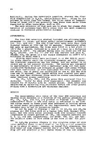
EXPERIMENTAL Ba 0 .7 Sr 0 3TiO 3 films were deposited on oxidized 6 inch Si-wafers by chemical solution deposition [12]. This method produced films typically 250 nm thick, as compared to 20-50 nm normally used for ULSI DRAM applications. Films were intentionally made thicker to exaggerate effects and aid the understanding of the plasma etching phenomena. The BST film was masked with photoresist (PR) and patterned by conventional optical lithography. The smallest features had dimensions of 0,7 gim. The dry etch of the BST layer was performed on a Lam Research Corporation TCPTM 9400SE. A conceptual drawing of the reactor design is shown in Fig. 1. A high density plasma is generated by inductively coupling RF power between a planar source coil and the plasma. The coupling occurs through a dielectric window which forms the top of the process chamber. Plasma densities RF Power in the range of 1010_1012 Supply 0n ions/cm 3 are produced for different plasma gas
chemistries at pressures
PlanarInductive Coil Dielectric Window
Par
1-100 mTorr.
obetween 0v
The ion density
:
is
controlled with the RF Controlled Pressure
Gas Composition
power applied to the TCP antenna. The ion energy can be changed
RF Power RFSupply
Bias Electrode
L
FMatch [Network
Substrate
with
applied
the
RF
to the
energy
wafer,
which was positioned . ,
Temperature Control
on
a temperature controlled chuck electrostatic (ESC).
Fig. 1 Schematic illustration for the Transformer Coupled Plasma (TCP) reactor showing the planar source coil and the temperature controlled wafer electrode.
RESULTS Physical etch
As a baseline, a physical sputter etch process with argon was evaluated. Removing the atoms physically by ion bombardment from the surface yields a thick, difficult to removable residue (fence) build up on the sides and top of the photoresist (see Fig. 2). Considering that the boiling points of the elements of barium strontium and titanium and their oxides are quite high [13], the residue is assumed to be sputtered BST.
110
The residue contaminates the wafer as well as the ins
Data Loading...