Application Areas of Epitaxially Grown Layer Structures
Epitaxial growth can be used for crystallization of thin film structures of different, metallic, semiconducting, and insulating material systems, including mixed systems like, e.g., metal—semiconductor or semiconductor-on-insulator device structures. The
- PDF / 1,129,002 Bytes
- 8 Pages / 439.37 x 666.142 pts Page_size
- 72 Downloads / 301 Views
Epitaxial growth can be used for crystallization of thin film structures of different, metallic, semiconducting, and insulating material systems, including mixed systems like, e.g., metal-semiconductor or semiconductor-on-insulator device structures. The epitaxially grown structures may be of very high perfection, satisfying the so-called device-quality demands. They are suitable for application in many branches of the "high technology" part of electronics, mechanics and materials engineering. However, the main application areas of epilayer structures are defined by solid state electronics, optoelectronics, and photonics [3.1-5].
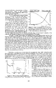
3.1 Low-Dimensional Heterostructures Crystallization of low-dimensional heterostructures (LDH) by epitaxy belongs to the most fascinating problems related to crystal growth of multilayer structures. Single or multiple quantum wells, quantum wires, and quantum dots (also called quantum boxes) create the LDH family. These structures are the constituent elements of mesostructure electronics [3.6-8]. MBE and MOVPE make possible the fabrication of heterostructures with composition varying on a spatial scale of one to 100 crystal-lattice constants. LDHs exhibit distinctive physical properties resulting from the occurrence of an intermediate size between two physical domains. The first is the microscale, or quantumeffects domain of lattice constants, or the de Broglie wavelength of the charge carriers. The second is the macroscale domain associated with quasi-classical motion of the charge carrier. The motion of carriers in a direction where potential barriers created by heterointerfaces confine them to an area that has a size belonging to the microscale, is strongly quantized, while the carriers motion in directions where no such confining barriers exist, is quasi-classical. Figure 3.1 illustrates the LDH family and the variation of the density of states of electrons with the increase of the quantization dimension in the LDH structures. The area of application of quantum well structures in semiconductor devices is already considerable, extending from high electron mobility transistors through double barrier resonant tunneling microwave diodes to quantum well lasers and quantum well intraband photo detectors [3.10]. The two other M. A. Herman et al., Epitaxy © Springer-Verlag Berlin Heidelberg 2004
36
3. Application Areas of Epitaxially Grown Layer Structures
EO bulk (conventional)
Ly
~ ffL' Lz
Lz
Lx
quantum film
quantum wue
quantum box
Fig. 3.1. The LDH structures (upper part) and the variation of the density of states of electrons (lower part) with the increase of the quantization dimension in LDH structures (taken from [3 .9 ])
groups of LDH structures, namely, quantum wires (QWR) and quantum dots (QD) are still under development and need further intensive investigations. However, the first optoelectronic devices with QWR structures [3.11] and QD structures [3.12] have been demonstrated, and some examples are presented in the next section. Here, we will describe an application of
Data Loading...


