Application of Amorphous GaN for Electroluminescence Device
- PDF / 202,703 Bytes
- 6 Pages / 612 x 792 pts (letter) Page_size
- 78 Downloads / 374 Views
Application of Amorphous GaN for Electroluminescence Device Tohru HONDA and Hideo KAWANISHI Department of Electronic Engineering, Kohgakuin University 2665-1 Nakano-machi, Hachiohji, Tokyo 192-0015, Japan
Abstract The vacuum evaporation of GaN thin films using GaN powder (5N) for GaN-based electroluminescence devices (ELDs) is reported. The crystal structures of the evaporated GaN layers were amorphous, which was confirmed from reflection high-energy electron diffraction (RHEED) patterns. Auger electron spectra revealed that the layers have excess Ga metal. Bluish-white light emission was observed from the GaN-based ELD under AC operation at RT. Although the emission intensity was weak, the electroluminescence spectra started from the band edge of h-GaN. 1. Introduction The III-V nitrides based on GaN have been applied for light-emitting diodes operating in green, blue violet and UV spectral regions [1,2]. Recently, electroluminescence devices (ELDs) using GaN as an emission layer have been investigated for application to flat displays [3,4]. It is necessary to establish fabrication techniques with low cost which realize a large area for the displays. However, GaN growth generally requires high temperatures for its synthesis. We consider that this technical issue must be overcome to separate the synthesis and deposition of GaN layers. Using concept described herein, we are investigating a deposition technique with a low substrate temperature. ELDs using GaN powder and ultrasonic dispersion for deposition have been reported [4]. In this case, the grain size of the GaN powder affects the lifetime of GaN-based ELDs. This technique is effective for fabricating emission layers of uniform thickness. In this study, we report vacuum evaporation using GaN powder for GaN-based ELDs with a uniform emission layer. We also report that amorphous GaN-based ELDs with bluish-white light I6.42.1
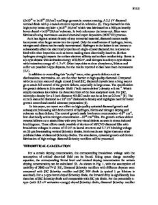
Deposition Rate (nm/h)
100 80 60 40
Tsub : RT 1 hour 2 hours 3 hours
20 0 900
1000
1100
Source Temperature (
℃)
1200
Fig. 1 Deposition rates of the films by vacuum evaporation.
emission were fabricated. 2. Experiments GaN powder (5N), which was synthesized using Ga metal and ammonia, was used for the vacuum evaporation as a source material. The deposition pressure was approximately 5x10⁻⁴ Pa. SiO2 glass substrates with Cr coating were used in this study. The source temperature was changed as a parameter from RT to 1200 °C and the substrate temperature was fixed at RT. The substrate temperature increased somewhat owing to the radiant heat from the source, but the temperature remained lower than 100 °C. The deposition rate as a function of source temperature is shown in Fig. 1. Solid squares, solid circles and open circles show growth times of 1, 2 and 3 hours, respectively. The deposition started at 900 °C and saturated at 1050 °C. The fabrication of thin films using a GaN source was possible by keeping the source temperature above 900 °C. With increasing deposition time up to three hours, the thickness of the films increased line
Data Loading...