Approaches For Reduction Of The Defect Density In Group III Nitride Based Heterostructures
- PDF / 5,131,143 Bytes
- 13 Pages / 612 x 792 pts (letter) Page_size
- 7 Downloads / 249 Views
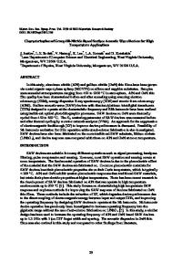
Approaches For Reduction Of The Defect Density In Group III Nitride Based Heterostructures T. S. Zheleva 1,2 F. Karoui 2, K. Kirchner 1, M. Derenge 1, K. A. Jones1. R. D. Vispute 3, T. Venkatesan 3 1 US Army Research Laboratory, Attn: AMSRL-SE-EM, 2800 Powder Mill Road, Adelphi, MD 20783, US 2 North Carolina State University, Box 7907, Raleigh, NC 27695-7907 3 Department of Physics, University of Maryland, College Park, MD 20742. Abstract Lateral epitaxial overgrowth (LEO), pendeo-epitaxy (PE), and solid-phase epitaxial recrystallization (SPER) are discussed as three approaches for reducing the defect density in group III nitride based heterostructures. Studies of the LEO GaN and PE GaN revealed, that a major factor for the defect reduction in the laterally overgrown regions is the change of the dominant growth direction - from vertical in the window regions to lateral in the regions over the mask or over the trenches, and the related threading dislocations lines redistribution. The mechanisms of defect reduction in LEO GaN and PE GaN are similar, although they arise through different process routes, and are related to the free-standing (PE) or quasi-free-standing (LEO) growth of GaN, and the associated stress redistribution. The stress distributions in the LEO and PE GaN heterostructures are calculated and compared with finite element modeling. Another approach for reduction of the defects is the SPER process and the related thermal activation for dislocation reactions and grain boundary mobility and migration. This approach is shown in the example of annealed AlN films. Introduction The increased interest in the phenomenon of lateral epitaxy in GaN based heterostructures in the past few years is mainly due to the notably improved performance of the electronic and optoelectronic devices [1-6] when built on the regions of lateral epitaxial overgrowth (LEO). Studies of LEO GaN on SiC and sapphire substrates [7-18], and pendeo-epitaxial (PE) GaN on SiC and Si substrates [19-27] have demonstrated substantially lower defect density, up to two to four orders of magnitude in the regions of lateral growth. In similarity to the PE growth of GaN on SiC substrates, PE approach for GaN growth on sapphire substrates has been applied, to achieve GaN material of lower defect density [28-31, 48,49]. In addition to the improved characteristics of the electronic devices when built on LEO and PE GaN, it is important to understand the fundamental mechanisms for reduction of the density of defects, which enables such drastic difference in the defect distribution. As it is common for thin film heterostructures one should take into account the lattice and thermal mismatch in the layers of the heterostructure as a main source of defect generation at the heterointerfaces and the subsequent defects propagation and interactions. Also, when the heterostructure is subjected to the particular thermal cycle during its fabrication, there is non-uniformly distributed stress and strain, associated with the defects and their interactions. A detailed
Data Loading...