Atomic and Electronic Structure of Interfaces at Sic Studied by Indirect Super Hrtem and Electron Spectroscopyn Imaging
- PDF / 312,404 Bytes
- 7 Pages / 595 x 842 pts (A4) Page_size
- 32 Downloads / 304 Views
R12.2.1
ATOMIC AND ELECTRONIC STRUCTURE OF INTERFACES AT SiC STUDIED BY INDIRECT SUPER HRTEM AND ELECTRON SPECTROSCOPYN IMAGING J. Y. Yan1, Hideki Ichinose2, Fu-Rong Chen1, J. J. Kai1, and Eriko Takuma2
1. Center of Electron Microscopy, Dept. of Engineering and System Science, National Tsing Hua University, Hsin Chu, Taiwan. 2. Department of Materials Science, School of Engineering, The University of Tokyo, Japan
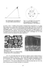
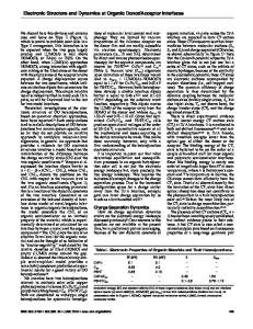
ABSTRACT Obtaining electronic and atomic structure of material simultaneously is very important for developing the nano-technology. In this paper, we demonstrate that atomic and electronic structure of an interface can be extracted with combination of Gerchberg-Saxton indirect microscopy and electron spectroscopy imaging (ESI) technique. Basically, Gerchberg-Saxton algorithm includes two projections. Projection in the real space is a maximum entropy (ME) de-convolution process and in reciprocal space is an amplitude substitution process. It has been shown that Gerchberg-Saxton algorithm can extend the structural resolution to near 0.1nm. An application case of Gerchberg-Saxton algorithm to solve the atomic structure for 3C-polytypic SiC boundary is shown. ESI spectrum processed by FFT interpolation, maximum entropy de-convolution and wavelet transformation allow us to extract 2-dimensional map of the sp2/sp3 with a sub-nanometer resolution. Grain boundary and interface at SiC are good candidates for this study, since the bond distance of Si-C is slightly less than 0.1nm which is not routinely resolvable using a FEG TEM and Si-L (99eV) and C-K-edges (283 eV) locate in a reasonable energy range. The resultant electronic structure can be compared with that calculated using WIEN97. An example of quantitative analysis on 2-dimensional sp3/sp2 map deduced from the C K-edge of ESI spectra acquired from 6H-SiC is given. INTRODUCTION Recent development in the nano-technology pushes the material scientist not only to determine atomic structure from our materials or devieces, but also to obtain the information of electronic structure in order to have a better control on the property of our nano-materials and devices. HRTEM and EELS are the two candidate techniques for the purpose of nona-area characterization of the atomic and electronic structures. In TEM, the structural information of high frequency in the image plane is cut off by the damping function of an objective lens and the phase information in the low frequency domain is modified by contrast transfer function (CTF) of a lens. The action of the objective lens usually, limits the resolution of HRTEM to slightly better than 0.2nm and makes the interpretation of HRTEM not obvious. We will first describe briefly the concept of the indirect microscopy using the Gerchberg-Saxton algorithm [1, 2] to recover the structural information up to 0.1 nm. An application case of Gerchberg-Saxton algorithm to solve the atomic structure for 3C-15R SiC twin boundary will be shown. Further, we introduce a set of signal processing methods to improve the quality of spectrum ext
Data Loading...