Atomistic Simulation of Flow Stress and Dislocation-Interface Interaction in Thin Metal Films
- PDF / 778,862 Bytes
- 6 Pages / 612 x 792 pts (letter) Page_size
- 54 Downloads / 398 Views
U9.4.1
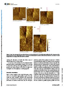
Atomistic Simulation of Flow Stress and Dislocation-Interface Interaction in Thin Metal Films E. S. Ege and Y.-L. Shen Department of Mechanical Engineering, University of New Mexico Albuquerque, NM 87131, U.S.A. ABSTRACT This study focuses on the atomistics of interface-mediated plasticity in thin metallic films. Molecular statics simulations are carried out to model the tensile stress-strain response of the free-standing and substrate-bonded films. In the free-standing film dislocation glide readily occurs, inducing slip steps at both surfaces of the film. The existence of an interface with the substrate constrains the dislocation motion in the film and restricts the slip steps to only the free surface. The propensity of film plasticity is dictated by the capability of atoms to slide along the interface. The flow stress of the film can be correlated with the dislocation activities obtained from the simulation. The propensity of spreading of relatively energetic atoms associated with the dislocation near the interface is also discussed. INTRODUCTION Substrate-bonded thin films derive their strength in part from the interfacial constraint caused by the underlying layer. This is manifested by the high plastic flow stress that can be carried by polycrystalline metal films on substrates compared to the case of free-standing films [1,2]. Prevailing theories for substrate strengthening and interface-constrained plasticity in metal films have invoked the concept of misfit dislocations left behind at the interface caused by dislocation gliding inside a crystal [1,3-5]. Such model is predicated upon the balance of the work done by the film stress and the stored energy of the interfacial misfit dislocation. However, there is a general lack of experimental evidence of misfit dislocations in recent electron microscopy examinations of aluminum and copper films [6,7]. This is not surprising because in most cases the metal film is in direct contact with an amorphous layer (such as oxidized silicon and silicon nitride barrier layer) of the substrate so a true “misfit” dislocation at the interface is not likely to exist. Clearly a different physical picture concerning interface-constrained plasticity for nonepitaxial crystalline films is needed. In this study we employ atomistic simulations to provide a mechanistic rationale for the substrate confinement effect. Attention is devoted to correlating incipient plasticity, defect mechanisms, and the overall stress-bearing capability. APPROACH The model system is a two-dimensional crystal with a close-packed structure. The initial configuration of atomic arrangement is shown in Fig. 1. To assist in triggering the onset of crystal plasticity and avoid brittle fracture, an artificial defect, in the form of a self-interstitial, is introduced in the model and allowed to equilibrate with its surrounding atoms before the loading steps commence. This technique enables the generation of dislocations inside the crystal for modeling purposes (see below), and the ductile elastic-plastic beh
Data Loading...