Atomistic study of the melting behavior of single crystalline wurtzite gallium nitride nanowires
- PDF / 2,811,943 Bytes
- 6 Pages / 585 x 783 pts Page_size
- 37 Downloads / 303 Views
Xiaotao Zu Department of Applied Physics, University of Electronic Science and Technology of China, Chengd, 610054, People’s Republic of China
Fei Gao and William J. Weberb) Pacific Northwest National Laboratory, Richland, Washington 99352 (Received 12 July 2006; accepted 21 November 2006)
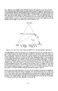
Molecular dynamic simulation was used to study the melting behavior of gallium nitride (GaN) nanowires with the Stillinger-Weber potential. Our results reveal that the melting of the nanowires starts from the surface and rapidly extends to the inner regions of nanowires as temperature increases. The melting temperatures increase to saturation values ∼3100 and ∼2900 K when the diameters of nanowires are larger than 3.14 and 4.14 nm for the nanowires with [100]- and [110]-oriented lateral facets, respectively. The saturated values are close to the melting temperature of bulk GaN. The low melting temperature of GaN nanowires with small diameter may be associated with the large surfaces of nanowires. I. INTRODUCTION
Single-crystalline, one-dimensional semiconductor nanostructures are considered to be one of the critical building blocks for nanoscale optoelectronics.1,2 To implement these nanoscale building blocks for electronic applications, their thermal and chemical stability have to be carefully considered because of the extremely small sizes and high surface areas. The melting behavior of metal nanoparticles has been demonstrated to be dramatically different from the bulk. Theoretical studies3 predict that the decrease in the melting temperature of a metal cluster is proportional to the inverse of the cluster diameter. This relationship has been validated experimentally4–6 and by computer simulations.7–10 Gallium nitride (GaN) is a high-temperature semiconductor material of considerable interest. It emits brilliant light and has been considered as a key material for the next generation of high-frequency and high-power transistors that are capable of operating at high temperatures. Single-crystalline GaN nanowires have already shown promise for realizing photonic and biological nanodevices such as blue light-emitting diodes11 and shorta)
Address all correspondence to this author. e-mail: [email protected] b) This author was an editor of this journal during the review and decision stage. For the JMR policy on review and publication of manuscripts authored by editors, please refer to http:// www.mrs.org/jmr_policy. DOI: 10.1557/JMR.2007.0095 742
J. Mater. Res., Vol. 22, No. 3, Mar 2007
wavelength ultraviolet nanolasers. 12,13 GaN-based nanowires have been synthesized using laser ablation,14 chemical vapor transport,15–20 or hydride vapor epitaxy.21 Most of these processes use Ga metal as the hightemperature vapor sources, but metals such as Fe, Ni, and Au have been used as initiators for vapor-liquid-solid nanowire growth. The most common growth direction for the nanowires is along the [001] crystalline axes with hexagonal crosssections,16,20,22–24 but other growth directions along [210] and [110] with triangular cross section
Data Loading...