Boron Segregation and Electrical Properties in Polycrystalline SiGeC
- PDF / 68,715 Bytes
- 6 Pages / 612 x 792 pts (letter) Page_size
- 21 Downloads / 309 Views
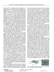
Boron Segregation and Electrical Properties in Polycrystalline SiGeC E. J. Stewart, M. S. Carroll*, and J.C. Sturm Center for Photonics and Optoelectronic Materials, Department of Electrical Engineering Princeton University, Princeton NJ * present address: Agere, Murray Hill, NJ ABSTRACT Previously, it has been reported that PMOS capacitors with heavily boron-doped polycrystalline SiGeC gates are less susceptible to boron penetration than those with poly Si gates [1]. Boron appears to accumulate in the poly SiGeC layers during anneals, reducing boron outdiffusion from the gate despite high boron levels in the poly SiGeC at the gate/oxide interface. In this abstract, we report clear evidence of strong boron segregation to polycrystalline SiGeC layers from poly Si, with boron concentration in poly SiGeC (Ge=25%, C=1.5%) increasing to four times that of adjacent poly Si layers. A separate experiment confirms that this result is not due to any SIMS artifacts. Electrical measurements of heavily in-situ doped single layer samples show that the conductivity of poly SiGeC is similar to poly Si and remains roughly constant with annealing at 8000C. However, in a two-layer sample where the poly SiGeC is initially lightly doped and subsequently heavily doped by diffusion by from an adjacent poly Si layer, conductivity appears lower than in poly Si. INTRODUCTION Heavily boron-doped polysilicon is typically used as the gate material for modern p-channel MOSFETs. Doping the polysilicon gate is usually achieved by ionimplantation using B or BF2+, followed by an anneal to activate the dopant and drive it throughout the gate. For devices with very thin gate oxides, boron can actually diffuse through the gate oxide and into the substrate during this activation anneal. This boron penetration into the substrate changes the doping in the channel, causing undesirable positive threshold voltage shifts in the device [2]. Previously, it has been shown that, by placing a thin layer of polycrystalline SiGeC at the bottom of the polysilicon gate, boron penetration can be greatly suppressed for both PMOS capacitors and p-channel MOSFETs [1,3]. It is well known that boron diffusion in single-crystal SiGeC can be over an order of magnitude slower than in single-crystal Si [4]. However, the polycrystalline SiGeC gate layers do not appear to be acting as boron diffusion barriers (grain boundary diffusion may be enhancing diffusion in poly vs single crystal SiGeC). Instead, boron diffuses through and appears to accumulate in the poly SiGeC layers during the anneal, giving a high dopant level at the gate/oxide interface [1,3]. This tendency for boron to segregate to poly SiGeC layers may be responsible for the reduced boron penetration. In this work, we present clear independent evidence of strong boron segregation to polycrystalline SiGeC layers. We also examine the electrical properties of boron in polycrystalline SiGeC layers subjected to annealing.
J6.9.1
EXPERIMENT Thermal oxides (~200 nm) were first grown on n-type substrates. Polycrystalline
Data Loading...