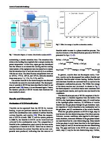
Carbon Nanotube-Based Vacuum Microelectronic Gated Cathode
- PDF / 1,655,358 Bytes
- 6 Pages / 414.72 x 648 pts Page_size
- 76 Downloads / 348 Views
ABSTRACT A vacuum microelectronic device containing carbon nanotube electron field-emitters was developed and tested. The gated cathode was fabricated using conventional microelectronics fabrication techniques and a final, self-aligned, in situ carbon nanotube growth step. To our knowledge, this is the first vacuum microelectronics device with carbon nanotube field-emitters grown in situ with a catalytic growth process. The turn-on voltage of the cathode was less than 20 volts and the emission current density at 50 volts was as high as 9 mA-cm- 2 . The fabrication process, device performance, manufacturing issues and cathode applications will be discussed. INTRODUCTION Robust cold electron sources or cold cathodes are required for the advancement of vacuum microelectronics. Many cold cathode structures, such as field emission cathodes,' energetic electron cathodes based on metal-insulator-metal and metal-oxide-semiconductor structures, 2 and negative electron affinity (NEA) cathodes,3',4 have been proposed and developed. Field emission cathodes based on metal or silicon cones are being further refined for application in field emission displays. In this paper, a novel field emission cathode based on carbon nanotube emitters that shows promise for low voltage operation and improved emission stability in poor vacuum is described. Carbon nanotubes are excellent electron emitters because of their small diameter and tip radius; carbon nanotubes are also mechanically stiff and electrically conductive.' Carbon nanotubes are chemically very stable, which should lead to a robust cathode, enabling operation in poor vacuum environments. Carbon nanotubes can be packed densely, enabling a high total emission current density, but with relatively low current load on individual nanotube emitters. This will minimize the Joule heating effect on the emitter that is typically observed in the arrays of needle and knife-edge emitters, reducing the danger of damage during operation. Smalley et al observed electron emission from a single nanotube at very low macroscopic electric field (800 V/cm).6 Heer et al. constructed a macroscopic electron source based on aligned carbon nanotubes.7 In Heer's cathode, carbon nanotubes, produced by a high intensity carbon arc in helium atmosphere,' are deposited on a substrate in an aligned fashion,9 and an SEM grid, separated from the carbon nanotube film by a 20-pm thick mica sheet, is used to extract electrons. Although carbon nanotubes are promising as robust electron emitters, currently available technology to produce carbon nanotubes is incompatible with the microelectronic 107
Mat. Res. Soc. Symp. Proc. Vol. 509 © 1998 Materials Research Society
processing needed to produce the cathodes and vacuum microelectronic devices. Currently carbon nanotubes are found in the soot from a carbon arc. They are produced in small quantity and in a very impure form. It is a challenge to cost-effectively fabricate micro field emission devices based upon these carbon nanotubes. In this paper, a novel fabrication
Data Loading...