Characterization of the Interface Between Metal Contacts and Epilayers of Doped Silicon Carbide
- PDF / 1,329,188 Bytes
- 5 Pages / 414.72 x 648 pts Page_size
- 69 Downloads / 446 Views
M.A. GEORGE*, D.J. LARKIN**, J. PETIT*, A. BURGER*, S. H. MORGAN* and W.E. COLLINS*, *Department of Physics, Fisk University, Nashville, TN 37208, and **NASA Lewis Research Center, Cleveland, OH 44135 ABSTRACT
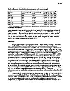
Aluminum contacts on chemical vapor deposited (CVD) SiC films were studied to examine variations in the chemical, morphological and electrical properties of the samples. Nitrogen and aluminum doped substrates were prepared to give n-type and p-type SiC epilayers respectively. These preparations were examined by surface sensitive spectroscopies and by atomic force microscopy (AFM). Samples were studied both before and after the deposition of aluminum films to compare differences between SiC(p++)/metal and SiC(n++)/metal contact interfacial properties. Aluminum has generally been found to have good adherence to the n+ epilayer but do not form good ohmic contacts, while metal films deposited on p+ epilayers have had poor adherence but have been found to provide better ohmic character. AFM images revealed nanometer sized clusters, attributed to excess Si on the n+ epilayers, while no clusters were observed on the p+ epilayers. XPS studies of the as-prepared samples indicated that the n+ epilayers had higher concentrations of oxides which may enhance adhesion. The chemical composition and morphology is discussed and correlated to the electrical properties obtained for the various samples. INTRODUCTION
In recent years, the Study of SiC has focused on methods to grow SiC for a wide range of applications including high temperature, high power devices' as well as optoelectronic devices2 . The preparation of good high quality epitaxial layers of SiC has been demonstrated by researchers at NASA Lewis and elsewhere, employing CVD methods3' 6. In particular, the preparation of high quality epilayers that can be undoped as well as p- or n-type doped during the deposition process to yield device grade films7' 8. In order to optimize subsequent development of devices, it is necessary to continue to examine the properties of cubic (3C) and hexagonal (411 and 6H) SiC grown layers. This includes the development of optimum metal contacts that have good adhesive properties and exhibit an ohmic character. This study involved the characterization of several samples that underwent various preparation conditions. These included samples that were selectively nitrogen doped and samples that were aluminum doped. The samples were studied both before and after the deposition of aluminum films to compare differences between SiC(p++)/metal and SiC(n++)/metal contact interfacial
properties. Atomic force microscopy (AFM) was utilized in this work to investigate the surfaces prior to deposition of aluminum. This was followed by additional measurements by x-ray photoelectron spectroscopy (XPS), and current-voltage (I-V) curves. The results enabled us to show a correlation between the adhesive and ohmic characteristics and the chemical species/defects that are formed on the surface or in the region just beneath the Al/SiC interface.
513
Mat
Data Loading...