Characterization study of GaN-based epitaxial layer and light-emitting diode on nature-patterned sapphire substrate
- PDF / 361,450 Bytes
- 7 Pages / 584.957 x 782.986 pts Page_size
- 1 Downloads / 368 Views
C.H. Kuo Institute of Lighting and Energy Photonics, National Chiao Tung University, Tainan City, Taiwan 30010, Republic of China
S.C. Hsu Department of Chemical and Materials Engineering, Tamkang University, New Taipei City, Taiwan 25137, Republic of China
C.Y. Liua) Department of Chemical and Materials Engineering, National Central University, Jhongli City, Taiwan 32001, Republic of China (Received 14 October 2011; accepted 28 December 2011)
Chemical wet etching on c-plane sapphire wafers by three etching solutions (H3PO4, H2SO4, and H3PO4/H2SO4 mixing solution) was studied. Among these etching agents, the mixing H3PO4/H2SO4 solution has the fastest etching rate (1.5 lm/min). Interestingly, we found that H2SO4 does not etch the c-plane sapphire wafer in thickness; instead, a facet pyramidal pattern is formed on the c-plane sapphire wafer. GaN light-emitting diode (LED) epitaxial structure was grown on the sapphire wafer with the pyramidal pattern and the standard flat sapphire wafer. X-ray diffraction and photoluminescence measurement show that the pyramidal pattern on the sapphire wafer improved crystalline quality but augmented the compressive stress level in the GaN LED epilayer. The horizontal LED chips fabricated on the pyramidal-patterned sapphire wafer have a larger light output than the horizontal LED chips fabricated on the standard flat sapphire wafer by 20%.
I. INTRODUCTION
Nowadays, the patterned-sapphire substrate techniques have been widely used in high-power GaN-based lightemitting diodes (LEDs), which are the most promising alternative light source for general lighting.1,2 With the breakthrough of the patterned-sapphire substrate technique, the efficacy of high-brightness GaN-based LEDs has been driven to a record high of 150 lm/W.3,4 The efficacy enhancement of GaN-based LEDs with the patterned-sapphire substrate technique generally attributes to the improvement in both light extraction efficiency and internal quantum efficiency.5–9 The regular patterns created on the sapphire substrate counteracts the effect of the total internal reflection at the GaN/sapphire interface.5 And, the enhancement in the internal quantum efficiency benefits from the reduction of threading dislocations by possible lateral growth of GaN epilayer on the patternedsapphire substrate.5,10–13 a)
Address all correspondence to this author. e-mail: [email protected] DOI: 10.1557/jmr.2012.24 J. Mater. Res., Vol. 27, No. 6, Mar 28, 2012
http://journals.cambridge.org
Downloaded: 26 May 2014
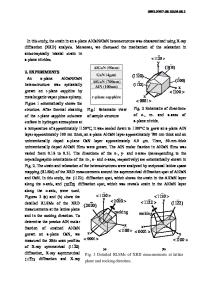
Numerous patterning features produced on the patternedsapphire substrate by either dry etching or wet etching processes, which includes circle cavities, square cavities, hemispheric bumps, and trenched stripes, have been studied.5,14–16 Yet, no matter what etching process is used to create the patterns, a hard mask lithographic process is required on the flat c-plane sapphire wafer. In this study, a mask-free wet etching process was used to produce a naturepatterned sapphire substrate (n-pss). Then, a metalorganic chemical vapor deposition
Data Loading...