Chemical Kinetics of Silicon-Rich Oxide Growth in an LPCVD Reactor
- PDF / 331,131 Bytes
- 7 Pages / 420.48 x 639 pts Page_size
- 23 Downloads / 220 Views
CHEMICAL KINETICS OF SILICON-RICH OXIDE GROWTH IN AN LPCVD REACTOR C.H. LAM' and K. ROSE Center for Integrated Electronics Rensselaer Polytechnic Institute Troy, New York 12181
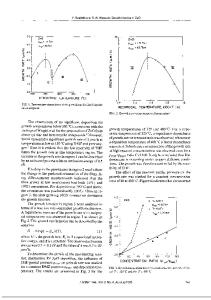
ABSTRACT The chemical kinetics of Silicon Rich Oxide (SRO) growth in a N20-SiH 4 LPCVD reactor has been studied at deposition temperatures from 610 to 6800 C and pressures from 0.4 to 0.5 torr. We can produce SRO films with a wide spectrum of input reactant ratios -y = [N201/[SiH 4] = 1 to 40. The dependence of film composition on Ychanges dramatically in a region around 7 = 2. Growth for - < 2 is consistent with the chemical kinetics of SIPOS growth. Growth for y> 20 can be explained by oxidation of silicon in the bulk of the growing SRO film. We can explain growth from 7 ; 4 to 20 by considering the chemical kinetics of possible binary surface reactions which may produce Si-Si or Si-O bonds. This allows us to accurately model the dependence of SRO growth rate in this region as a function of 7, pressure, and deposition temperature. INTRODUCTION By increasing 7, the ratio of [N2 0] to [SiH41, in an LPCVD reactor one can produce SiO, films with increasing oxygen content. At low -y these films approach polysilicon and are described as SIPOS, Semi-Insulating PolySilicon. SIPOS is commonly used as a surface passivant for high-voltage devices [1]. For high 7 one approaches SiO2, producing OffStoichiometry Oxides (OSO) which can be used as insulating layers in EAROM technology [2]. At intermediate 7 one produces Silicon-Rich Oxides (SRO) which are useful as injecting layers in EAROM technology [3]. We report the growth kinetics of SRO films using silane (10% in nitrogen) and nitrous oxide as reactant gases. Deposition temperatures were varied from 610 to 680'C, deposition pressures from 0.4 to 0.5 torr. Growth and measurement techniques are discussed in the next section. This is followed by a comparison of our low 7 results with the model of Hitchman and Kane [4] for SIPOS growth. An alternative model is developed to explain growth at higher values of -1. Anomalous deposition around 7 ; 2 is noted. GROWTH AND MEASUREMENT TECHNIQUE Two-inch p-type-silicon wafers were RCA cleaned within 24 hours prior to film deposition. This was followed by a 30-second dip in 10% aqueous HF to remove native oxide before the wafers were loaded into our reactor. The two heating zones toward the loading door were maintained at the same temperature, while the heating zone toward the pump and was maintained at a slightly lower temperature to avoid excessive deposition on the tube wall. 1
Now at IBM, 1000 River Road, Essex Junction, Vermont 05452
Mat. Res. Soc. Symp. Proc. Vol. 131. t1989 Materials Research Society
282
Wafers were loaded horizontally in the center zone of the reactor. Temperature variation in this zone was less than 2°C. In our reactor, film thickness variation across horizontally loaded wafers was typically around 5% compared to as much as 50% from the center to the periphery for vertically loaded wafers. The loading configuration had little effec
Data Loading...