Chemical-Vapor-Deposited Tungsten for Vertical Wiring
- PDF / 11,107,157 Bytes
- 7 Pages / 576 x 777.6 pts Page_size
- 68 Downloads / 442 Views
wires. The reduction in size increases the aspect ratio of these features for the same dielectric thickness. Conventional physical vapor deposition (PVD) techniques such as sputtering are unable to fill high aspect-ratio contacts/vias with alu-
minum conformally, as shown in Figure 1. This poor conformity is attributed to the shadowing effect by alreadydeposited nondirectional sputtering atoms and leads to void formation and open failures. Chemical vapor deposition (CVD) is a solution for achieving conformal filling. This is a prime reason why CVD has been investigated since the 1980s and why a large number of metals have been proposed. Above all, because tungsten as a refractory metal has high resistance to electromigration (EM) failures and tungsten hexafluoride (WF6) as a source gas has some advantages in manufacturing, for example, high vapor pressure (boiling point = 17.4°C) and purity, W-CVD with WF6 based on H 2 or SiH4 reduction has been widely studied. 1 Blanket W-CVD has been used for actual via-hole filling for 0.5-/xm devices. Figure 2 shows a cross-sectional view of five-level interconnects using W plugs in
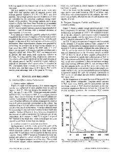
Vertical Wiring Process
Cleaning
Sputter Ti
Sputter TiN
Sputter Al
y
1! Cleaning
Cleaning
Sp.-Ti
////// jj
Sp.-TiN Blanket W Etch-back Sputter Al
Selective W
Sputter TiN
Sputter Al
Figure 1. Schematic diagram of process flow of vertical wiring using conventional sputtering, blanket W-chemical vapor deposition (CVD), and selective W-CVD, along with their SEM cross-sectional views.
46
MRS BULLETIN/NOVEMBER 1995
Chemical-Vapor-Deposited Tungsten for Vertical Wiring
0.35-/j.m devices.2 Another advantage of W-CVD is that W deposits selectively into via holes if a low flow-rate ratio of reductants to WF6 is used. Since selective W-CVD does not require any metal liner such as titanium-nitride (TiN) or etch back for the plug processes, there is a high potential to fabricate multilevel interconnects for deep-quarter-micron devices while lowering process cost and complexity. In this article, deposition characteristics and recent studies of both blanket and selective W-CVD are described. Blanket W-CVD Because of the improved productivity and the ability to fill via holes, the combination of blanket W-CVD and the etch-back process is currently the best alternative to sputtered Al. For blanket W-CVD, the following hydrogen reduction reaction of WF6 is usually used: WF6(g) + 3H2(g) = W(s) + 6HF(g).
(1)
The high step coverage obtained by blanket W-CVD and good filling of via holes without the leaving of voids are explained by the rate-limited reaction kinetics with an activation energy of 0.71-0.75 eV, which is determined by the dissociation of H 2 into atomic H.34 The deposition rate increases as the square root of the H 2 partial pressure. For high throughput and high film quality (smooth surface and complete step coverage), several tens of Torrs (—80 Torr) total pressure have been used for the blanket W-CVD process in recent manufacturing (Figure 3).5~7 Moreover, to ensure the nucleation
Data Loading...