Comparative study on electrical and microstructural characteristics of ZrO 2 and HfO 2 grown by atomic layer deposition
- PDF / 1,597,129 Bytes
- 8 Pages / 612 x 792 pts (letter) Page_size
- 97 Downloads / 383 Views
Krishna C. Saraswat Department of Electrical Engineering, Stanford University, Stanford, California 94305
Paul C. McIntyre Department of Materials Science and Engineering, Stanford University, Stanford, California 94305 (Received 14 June 2005; accepted 15 August 2005)
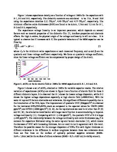
Ultra-thin ZrO2 and HfO2 dielectric films grown by atomic layer deposition (ALD) are quite promising materials for gate dielectric applications in future transistors, and they exhibit significantly different as-grown microstructures: polycrystalline and amorphous phases, respectively. However, under the identical deposition conditions, both metal oxides show surprisingly similar capacitance–voltage (C–V) characteristics as a function of film thickness, implying that the identities and densities of fixed charge and bulk trapping charge are similar. Factors other than the film microstructure, such as concentration of impurities incorporated during the film deposition, are believed predominantly to control important C–V characteristics. Only the dielectric constant appears to depend significantly on the identity of the dielectric material. It is found that the dielectric constant of ALD-HfO2 (∼20) is significantly lower than that of ZrO2 (∼30) due to the differences in microstructure and also atomic density of the film. In terms of the leakage current characteristics, the effective potential barrier heights between Pt and these two dielectric films are identical (∼2.3 eV) within the experimental uncertainty. Implications for the electrode/dielectric interface electronic structure are discussed.
I. INTRODUCTION
Silicon dioxide has been used as the primary gate dielectric material in CMOS (complementary metal-oxidesemiconductor) FET (field effect transistor) devices since 1957 due to its superior material and electrical properties.1 While the desire to enhance device speed continues to drive the dielectric thickness downward, it has been demonstrated, both experimentally2 and theoretically,3 that a minimum of about 0.7 nm of SiO2 is required to obtain the bulk properties of the oxide. Furthermore, several research groups have reported that scaling of CMOS structures with SiO2 gate oxides thinner than 1–1.2 nm results in no further gains in transistor drain current, and thus the practical limit of the SiO2 thickness is slightly larger than 0.7 nm.4 As the lateral dimensions of CMOS transistors decrease and higher switching speeds are required, scaling laws prescribe that
a)
Address all correspondence to this author. e-mail: [email protected] DOI: 10.1557/JMR.2005.0394 J. Mater. Res., Vol. 20, No. 11, Nov 2005
http://journals.cambridge.org
Downloaded: 09 Feb 2015
the SiO2 gate dielectric thickness must be decreased to less than 1.5 nm for a device with a 0.1-m channel length. However, with the reduction of the SiO2 thickness, the leakage current across the gate dielectric increases enormously through direct tunneling and cannot meet the maximum allowable leakage current density (∼1 A/cm2) for optimal transistor operation.5 As a result, high leakage
Data Loading...