Comparison of Novel Chlorine, Bromine and Iodine Plasma Chemistries for Anisotropic Trench Etching In GaN, InN and Ain
- PDF / 387,558 Bytes
- 6 Pages / 414.72 x 648 pts Page_size
- 105 Downloads / 294 Views
hick and were nominally undoped(n - 6x1016cm- 3 for GaN, n - 10 2 0Cm- 3 for InN and resistive, > 108'erm, for AIN). The samples were patterned with various mask materials, including photoresist or SiNx. Etching was performed in a Plasma Therm 790 system utilizing a 3 turn coil ICP source operating at 2MHz and powers up to 1500W. The samples were thermally bonded to a Si carrier wafer that was mechanically clamped to a He backside cooled, rf powered (13.56MHz, 450W) chuck. The B13 and BBr 3 were contained in a vacuum vessel heated to -45°C to increase their vapor pressure - B13 is a solid with a melting point of 40'C, while BBr 3 is a liquid with a boiling point of 91'C. We generally added Ar to the gas load(total flow of all gases was held constant at 10 standard cubic centimeters per minute, sccm) to facilitate plasma ignition and enhance the physical component of the etching and maintained process pressure at 5mTorr. Etch rates were obtained from stylus profilometry measurements of the features, while scanning electron microscopy(SEM) and atomic force microscopy(AFM) were used to examine
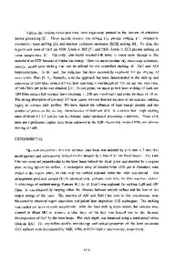
surface morphology. RESULTS AND DISCUSSION (a) C12/Ar Plasma Etching Figure 1 shows the nitride etch rate and selectivity data as a function of plasma composition in C12/Ar discharges, with -100V dc self-bias, 2mTorr pressure and 750W ICP source power. The rf chuck power was adjusted at each composition to keep dc bias constant. There are maxima in the etch rates at specific plasma compositions. This is most likely related to the existence of optimal neutral-to-ion ratios that provide sufficient C12 surface coverage and reaction, and subsequent etch product desorption. 2000 -10. Ci2/Ar
750W ICP
- 1600
./-ý/
-100V dc
K
1200
2mTorr
\\
800
:/
A/-
/
S400
A,
4-N A
0
I
.
0
20
--
InN/A IN
IInN
40
I 60
80
10.1 100
0
Percent Cl2
20
40
60
80
100
Percent Ci2
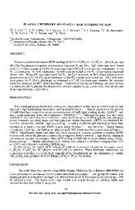
Figure 1.Nitride etch rates(left) and etch selectivities for InN/A1N and InN/GaN(right) in C12/Ar discharges(750W source power, -100V dc self-bias, 2mTorr) as a function of plasma composition. Figure 2(left) shows that at fixed dc self-bias(-10OV) and plasma composition(10C12/5Ar), increasing the ICP source power increases the nitride etch rates by increasing the ion flux and the atomic chlorine density. The results for InN are similar to what we observe for InP in that there is a sharp rise in etch rate above a particular source power[ 11], which we ascribe to the prevention of formation of an InC13 selvedge layer which normally retards further etching[12,13]. Further increases in flux(corresponding to source powers above 1000W) do not 502
increase the InN(or InA1N) etch rate, which at that point may be limited by C12 arrival at the surface. The other materials show a general trend of increasing etch rate across the entire range of ICP source powers. 5000 A .• 4000
10C12/Ar
/
dc Bias -100V
/
/
2mTorr
*3000
S2000
--
---/
10
AIN
Fl
.•
GaN
/
/
0
S~-4-I-InN/GaN 0
400
800
1200
1600
0
ICP Source Power (W)
400
800
1200
1600
I
Data Loading...