Computational modeling of nanosecond time-scale charge carrier dynamics in organic semiconductors
- PDF / 1,638,275 Bytes
- 6 Pages / 612 x 792 pts (letter) Page_size
- 26 Downloads / 295 Views
Computational modeling of nanosecond time-scale charge carrier dynamics in organic semiconductors Brian Johnson1, Keshab Paudel1, Oksana Ostroverkhova1 1
Oregon State University, Corvallis, OR, United States
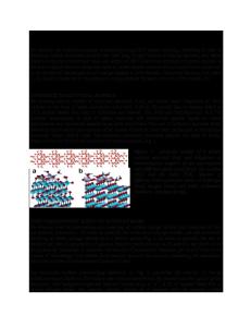
ABSTRACT We present a study of photoinduced charge carrier dynamics in single crystals and polycrystalline thin films of a functionalized fluorinated anthradithiophene (ADT) derivative, ADT-TES-F, combining measurements of time-resolved photocurrent with computational modeling. Simulations revealed two competing charge generation pathways: ultrafast charge separation and nanosecond (ns) time-scale exciton dissociation. Single crystals exhibited significantly enhanced fast charge photogeneration and charge carrier mobilities, as well as lower charge trap densities and free hole-trapped electron recombination, as compared to thin films. At sub-ns time scales after photoexcitation, the light intensity dependence of the photocurrents obtained in single crystals was determined by the carrier density-dependent recombination. At longer time scales, and at lower intensities, taking into account carrier concentration-dependent mobility improved agreement between numerically simulated and experimentally measured photocurrent data. INTRODUCTION Organic semiconductors are of interest for (opto)electronic applications due to their ease of fabrication, low cost, and tunable properties. A considerable research effort has been applied to characterizing charge photogeneration and transport, as well as structure-property relationships, in small-molecule and polymeric materials.1,2 One promising class of organic materials is solution-processable small-molecule organic semiconductors with high charge carrier mobilities and strong photoresponse. Examples of such materials are functionalized anthradithiophene (ADT) derivatives which display fast photoresponse, thin-film transistor (TFT) charge carrier (hole) mobilities of ~1.5 cm2/Vs in spin-cast films, and high photoconductive gains under continuous wave excitation.3,4 However, understanding of mechanisms of enhanced charge photogeneration and charge transport in these materials is lacking and is necessary for guiding design of improved materials. To address these issues, we developed in our previous work a numerical model which allowed us to analyze photocurrent dynamics in polycrystalline thin films of functionalized ADT derivatives5–7 and bulk heterojunctions with the ADT donor. In particular, we quantified the contributions of various charge generation pathways and of charge carrier transport, trapping, and recombination properties to experimentally measured timeresolved photocurrents (TPCs). Here, we extend this work to single crystal devices, which are good model systems for studies of intrinsic properties of the material, and compare various parameters pertaining to photoinduced charge carrier dynamics in single crystals and thin films of a fluorinated ADT derivative functionalized with triethylsilylethynyl (TES) side groups, ADTTES-F (Fig. 1b, inset). One of the tests of r
Data Loading...