Consecutive Selective Chemical Vapor Deposition of Copper and Aluminum from Organometallic Precursors
- PDF / 1,956,189 Bytes
- 6 Pages / 420.48 x 639 pts Page_size
- 21 Downloads / 353 Views
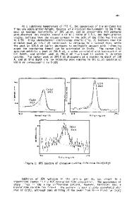
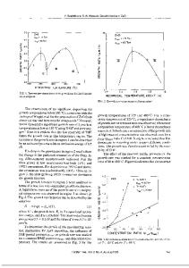
CONSECUTIVE SELECTIVE CHEMICAL VAPOR DEPOSITION OF COPPER AND ALUMINUM FROM ORGANOMETALLIC PRECURSORS. Stephen M. Fine*, Paul N. Dyer*, and John A. T. Norman** *Air Products and Chemicals, Inc., 7201 Hamilton Boulevard, Allentown, PA 18195 "**SchumacherCo., 1969 Palomar Oaks Way, Carlsbad, CA 92009. ABSTRACT For the next generation of integrated microcircuits, there exists a need in the electronics industry for high conductivity, electromigration resistant metallization that can be deposited selectivity by chemical vapor deposition techniques. This paper describes a new process for depositing copper/aluminum metallization selectively onto diffusion barrier surfaces in two consecutive steps. First copper is selectively deposited by OMCVD onto a patterned diffusion barrier surface using a Cu(I)(hfac)(olefin) precursor. Selective copper deposition onto tungsten or titanium nitride is achieved at 150'C and 100 mtorr. Aluminum is then selectively deposited onto copper using trimethylaminealane as the OMCVD precursor. Trimethylaminealane gives good selectivity for aluminum deposition onto copper surfaces over a temperature range of 100-120'C without the use of a surface activating agent. A small amount of copper diffuses into the as deposited aluminum layer at the low deposition temperature. Complete diffusion of copper into aluminum is achieved by a rapid thermal anneal at a higher temperature. The selectivity of aluminum deposition onto copper surfaces is far superior to that observed for aluminum deposition onto other metal surfaces. INTRODUCTION Aluminum/copper alloys have become the metallization of choice for very large scale integrated circuits (VLSI). The most common methods for depositing the alloy are magnetron sputtering or other physical vapor deposition (PVD) techniques. However, as the feature size of ultra-large scale integrated circuits (ULSI) continues to decrease to the sub 0.5 gtm regime, it becomes increasingly difficult to successfully use PVD metallization. PVD is largely a line-of sight technique and has difficulty conformally coating < 0.5 gtm high aspect ratio features. This limitation of PVD has created a growing interest in CVD techniques. CVD is an inherently conformal process and excellent step coverage is possible. Also, since CVD can be catalyzed by portions of the substrate surface, selective deposition is possible. The production of
Data Loading...