Controtle Substitutional Doping of Cdte Thin Films and Cd 1-x Mn x Te-CdTe Superlattices
- PDF / 419,081 Bytes
- 8 Pages / 420.48 x 639 pts Page_size
- 104 Downloads / 398 Views
CONTROTLE
R.N.
BICKNELL,
N.C.
SUBSTITUTIONAL DOPING OF CdTe THIN FILMS AND Cd IxMn xTe-CdTe SUPERLATTICES.
GILES,
AND J.F. SCHETZINA
Department of Physics, North Carolina State University Raleigh, NC 27695-8202 ABSTRACT
We report the successful substitutional doping of CdTe epilayers grown by a new technique: photoassisted molecular beam epitaxy, in which the substrate is illuminated during the film deposition process. This new technique was found to produce dramatic changes in the electrical transport properties of the epilayers. In particular, highly conducting n-type and p-type CdTe films have been grown using In and Sb as n-type and p-type dopants,respectively. Photoassisted MBE has also recently been employed to produce for the first time highly conducting CdMnTe epilayers and Cd1 -xMnxTe-CdTe superlattices.
INTRODUCTION
CdTe is one of the most promising II-VI semiconductor compounds for applications in the areas of optoelectronics, gamma-ray detection and solar energy conversion [1-2]. There is at present also, considerable interest in
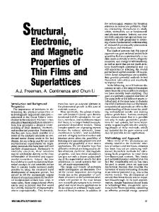
the use of CdTe substrates and buffer layers for the growth of HgCdTe, an important infrared material [3-5]. The recent work of Kolodziejski et al. [6] and Bicknell et al. [7], who have grown multiple quantum well structures of Cd Mn Te-CdTe has further sitmulated interest in thin film CdTe. StimulateA emission has also been reported from optically pumped Cd1 Mn Te-CdTe, Cd 1 xMn xTe-Cdl Mn Te, and Zn
Mn Se-ZnSe multilayer structures f7-81.
Future applicatlo s gf CdTe,
HgRafe,xand Cd Mn Te-CdTe superlattices will require the precise control of their electronic transport properties through substitutional doping. Incorporation of substitutional dopants in CdTe films grown by conventional molecular beam epitaxy (MBE) generally leads to poor activation of the dopant species [9]. Similar results have been obtained in bulk CdTe:In samples and has been attributed to self-compensation [10]. The development of II-VI semiconductor applications has been severely limited because of their strong tendencies towards self-compensation. At North Carolina State University, we have developed a new doping technique, compatible with molecular beam epitaxy, which allows introduction of selected dopant species during thin film growth: photoassisted MBE. In the photoassisted MBE process, the substrate is illuminated during the thin film deposition. The incident photon beam provides high energy, low momentum particles (photons) at the film growth surface in order to influence surface chemical reactions during film growth. This may be accomplished in several ways: through enhancement of surface migration of constituent atoms, modification of surface bonds, conversion of surface molecules into atoms, etc. The net result is that the photoassisted process promotes the incorporation of the substitutional dopant species at the proper tetrahedrally coordinated lattice sites.
Mat. Res. Soc. Symp. Proc. Vol.90.
1987 Materials Research Society
164
A technique similar to photoassisted MBE has b
Data Loading...