Critical Current Density of Narrow Superconducting Thin Films Fabricated by Laser Ablation Techniques
- PDF / 672,707 Bytes
- 4 Pages / 420.48 x 639 pts Page_size
- 29 Downloads / 363 Views
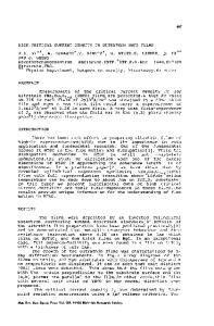
CRITICAL CURRENT DENSITY OF NARROW SUPERCONDUCTING THIN FILMS FABRICATED BY LASER ABLATION TECHNIQUES L. W. SONG, Y. H. KAO, Q. Y. YING, J. P. ZHENG, H. S. KWOK, Y. Z. ZHU, AND D. T. SHAW New York State Institute on Superconductivity and State University of New York at Buffalo, Buffalo, New York 14260 ABSTRACT The variations of critical current density J. of narrow Y-Ba-Cu-O films as a function of temperature and magnetic field are investigated. Films with thickness of 150-200 nm and width of 20-100 gim were prepared by laser ablation and laser etching. For t (=T/Tc) < 0.75, the temperature dependence of Jc shows a (1- t) linear behavior, in sharp contrast to that of a Josephson junction. Near Tc, Jc varies with (1- t)n where n=3/2 or 2 depending on the morphology of films. The magnetic field dependence of Jc above a characteristic field value Hc' can be described by a model based on flux creep. Thin films of high-Tc superconductors often exhibit properties significantly different from that of bulk materials. Of considerable interest is the high critical current density Jc and c-axis oriented structure found in thin film samples. However, the correlations between the film morphology and superconducting behavior are unclear, and the inevitable granular structures are believed to play an important role in affecting the physical properties. In this paper, we report results obtained with narrow thin films of Y-Ba-Cu-O fabricated by using laser ablation and laser etching techniques[1,2]. Although it is expected that these films contain grain boundaries, the variations of Jc with temperature and magnetic field are quite different from those observed in films with a single grain or across a grain boundary[3]. Thin film samples used in the present study were prepared by laser ablation on ZrO 2 single crystal substrates. Details of this ablation technique were described elsewhere[I]. The substrate temperature was maintained at 600-650 OC, with oxygen partial pressure at approximately 0.1 millitorr. The separation between the target and substrate was -20 cm and the film deposition rate was about 5 nm per second. Typical film thickness is between 150 and 200 nm. Narrow constriction of the film, or microbridge, was fabricated by Ar-laser patterning[21. The length of the narrow bridge is 1 mm, and the width is about 20 gm for sample 1 and 100 gm for sample 2. The films were characterized by x-ray powder diffraction, SEM and EDAX. The transition temperature Tc was determined from resistive transition by the standard four-probe measurements. Jc was determined from the current density at the onset of a voltage equal to 1 gV. The SEM micrograph is shown in Fig. 1. Sample 1 shows a porous structure with
Mat. Res. Soc. Symp. Proc. Vol. 169. ©1990 Materials Research Society
892
1
Iim
Fig. 1 SEM micrographs for (a) sample 1, (b) sample 2. grains of size around 0.5 gm, and sample 2 is less porous and with a somewhat smaller grain size. EDAX measurements indicate that both samples have very uniform Y-Ba-Cu-O ("123") composition. X-
Data Loading...