Crystal Structure Change with Applied Electric Field for (100)/(001)-oriented Polycrystalline Lead Zirconate Titanate Fi
- PDF / 738,564 Bytes
- 6 Pages / 612 x 792 pts (letter) Page_size
- 14 Downloads / 277 Views
Crystal Structure Change with Applied Electric Field for (100)/(001)-oriented Polycrystalline Lead Zirconate Titanate Films Ayumi Wada1, 2, Yoshitaka Ehara1, Shintaro Yasui1, Takahiro Oikawa1, Mitsumasa Nakajima1, Megu Wada1, P. S. Sankara Rama Krishnan1, Soichiro Okamura2, Ken Nishida3, Takashi Yamamoto3, Takeshi Kobayashi4, Hitoshi Morioka5, and Hiroshi Funakubo1 1
Department of Innovative and Engineered Materials, Tokyo Institute of Technology, Yokohama, Kanagawa 226-8502, Japan 2 Department of Applied Physics, Faculty of Science, Tokyo University of Science, Shinjuku-ku, Tokyo 162-8601, Japan 3 Department of Communications Engineering, National Defense Academy of Japan, Yokosuka, Kanagawa 239-8686, Japan 4 National Institute of Advanced Industrial Science and Technology (AIST), Tsukuba, Ibaraki 305-8564, Japan 5 Bruker AXS K. K., Yokohama, Kanagawa 221-0022, Japan
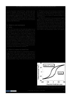
ABSTRACT Crystal structure change with an applied electric field was investigated by Raman spectroscopy and X-ray diffraction (XRD) for the 1 m-thick (100)/(001) one-axis oriented tetragonal Pb(Zr0.3Ti0.7)O3 films prepared on Pt-covered (100) Si substrates by chemical solution deposition technique. As-deposited films were under the strained condition in good agreement with the estimation from the thermal strain applied under the cooling process after the deposition from the Curie temperature to the room temperature. This strain was ascertained to be relaxed by an applied electric field in accompanying with the dramatic increase of the volume fraction of (001) orientation. These results demonstrate the importance of the crystal structure measurement not only as-deposited films, but also after applied electric field, such as after poling.
INTRODUCTION Films of lead zirconate titanate, Pb(Zr,Ti)O3, deposited on Si substrates have been widely investigated for the applications of microelectromechanical systems (MEMS) due to their superior piezoelectricity [1]. (100)/(001) one-axis-oriented films are reported to have a large piezoelectric response and are widely investigated [2]. Piezoelectric properties of Pb(Zr,Ti)O3 films are known to be strongly depended on the crystal structure, for example strain state of the films [3]. Therefore, the estimation of the strain state in the films on each device fabrication process is very useful to make MEMS device with high reproducibility. Strain state of the films is known to be strongly affected by the existence of the substrates [4]. Especially, in-plane strain is the primly one that is directly affected by the substrate that result in the nonsymmetrical strain along in-plane and out-of-plane strain directions of the substrates surface. X-ray diffraction (XRD) has been widely used for the crystal structure studies of thin films. Out-of-plane strain information can be obtained from the conventional – 2 scans, while the in-plane strain for the out-of-plane one-axis film is measured by the grazing incidence in-
plane diffraction (IP-GID) method. The conventional -2 scans offer a spatial resolution of the ord
Data Loading...