Crystalline Perfection of Epitaxial Structure: Correlations with Composition, Thickness, and Elastic Strain of Epitaxial
- PDF / 1,205,555 Bytes
- 6 Pages / 612 x 792 pts (letter) Page_size
- 1 Downloads / 284 Views
1167-O07-04
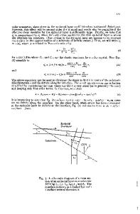
Crystalline Perfection of Epitaxial Structure: Correlation with Composition, Thickness, and Elastic Strain of Epitaxial Layers Balakrishnam R Jampana1, Nikolai N Faleev2, Ian T Ferguson3, Robert L Opila1, Christiana B Honsberg4 1 Material Science and Engineering, University of Delaware, Newark, Delaware 19716, USA 2 Electrical and Computer Engineering, University of Delaware, Newark, Delaware 19716, USA 3 School of Electrical and Computer Engineering, Georgia Institute of Technology, Atlanta, Georgia 30332, USA 4 Electrical Engineering, Arizona State University, Tempe, Arizona 85287, USA ABSTRACT Crystalline perfection of InGaN epi-layers is the missing design parameter for InGaN solar cells. Structural deterioration of InGaN epi-layers depends on the thickness, composition and growth conditions as well. Increasing the InGaN epi-layer thickness beyond a critical point introduces extended crystalline defects that hinder the optical absorption and electrical properties. Increasing the InGaN composition further reduces this critical layer thickness. The optical absorption band edge is sharp for III-nitride direct band gap materials. The band edge profile is deteriorated by creation of extended crystalline defects in the InGaN epitaxial material. The design of InGaN solar cells requires the growth of epi-layers where a trade off between crystalline perfection and optical absorption properties is reached. INTRODUCTION InGaN alloys with band gap variability in the 0.7 to 3.4 eV are used commercially to make blue and UV LEDs and lasers. This band gap range makes it possible to develop multiple junction solar cells to span most of the solar spectrum and achieve ultra high efficiencies [1, 2]. Wide band gap (> 2.2 eV) InGaN solar cells are being currently explored, owing to the band gap limitation of other materials. InGaN homo-junction solar cells with 2.0 V open circuit voltage have been demonstrated under AM1.5 illumination [3], but the short circuit current in these solar cells is low. InGaN p-i-n solar cells and quantum well solar cells have also been demonstrated [4, 5] but in most cases the open circuit voltage or the short circuit currents are low. The degradation of all these solar cells can be correlated back to the crystalline quality of the InGaN epitaxial material. InGaN epitaxial material has been studied for almost two decades now. Most of the research was focused on development of LEDs and lasers. The thickness of the active layer is less than 10 nm in these device structures. The solar cells require thicker InGaN material (> 100 nm) determined by the absorption coefficients. The issues originating with growth of thicker InGaN material and their effect on device performance have not been addressed extensively in the past research. In this paper, we present the spatial distribution of crystalline defects in InGaN epitaxial layers and correlate these with the observed optical absorption properties. The paper presents the observed crystalline quality results for In0.12Ga0.88N epi-layers with increas
Data Loading...