Crystallographic orientation effect on cutting-based single atomic layer removal
- PDF / 3,389,326 Bytes
- 14 Pages / 595.276 x 785.197 pts Page_size
- 78 Downloads / 360 Views
RESEARCH ARTICLE
Wenkun XIE, Fengzhou FANG
Crystallographic orientation effect on cutting-based single atomic layer removal
© Higher Education Press 2020
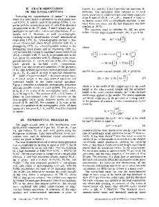
Abstract The ever-increasing requirements for the scalable manufacturing of atomic-scale devices emphasize the significance of developing atomic-scale manufacturing technology. The mechanism of a single atomic layer removal in cutting is the key basic theoretical foundation for atomic-scale mechanical cutting. Material anisotropy is among the key decisive factors that could not be neglected in cutting at such a scale. In the present study, the crystallographic orientation effect on the cutting-based single atomic layer removal of monocrystalline copper is investigated by molecular dynamics simulation. When undeformed chip thickness is in the atomic scale, two kinds of single atomic layer removal mechanisms exist in cutting-based single atomic layer removal, namely, dislocation motion and extrusion, due to the differing atomic structures on different crystallographic planes. On close-packed crystallographic plane, the material removal is dominated by the shear stress-driven dislocation motion, whereas on non-close packed crystallographic planes, extrusion-dominated material removal dominates. To obtain an atomic, defect-free processed surface, the cutting needs to be conducted on the close-packed crystallographic planes of monocrystalline copper. Keywords ACSM, single atomic layer removal mechanism, crystallographic orientation effect, mechanical cutting, Manufacturing III
Received May 10, 2020; accepted July 1, 2020
✉
Wenkun XIE, Fengzhou FANG ( ) Centre of Micro/Nano Manufacturing Technology (MNMT-Dublin), University College Dublin, Dublin 4, Ireland E-mail: [email protected] Fengzhou FANG State Key Laboratory of Precision Measuring Technology and Instruments, Centre of Micro/Nano Manufacturing Technology (MNMT), Tianjin University, Tianjin 300072, China
1
Introduction
1.1
Scope of atomic and close-to-atomic scale cutting
Atomic and close-to-atomic scale manufacturing (ACSM), i.e., Manufacturing III [1], aims to realize the manufacture of processed surfaces with atomic-scale form accuracy or feature size via material removal, transformation, and addition at atomic and close-to-atomic scales [2]. It will involve the fundamental study, technological development, and engineering applications of the controlled removal, addition, and migration of targeted atoms in Manufacturing III [2], where the external energy directly impacts individual atoms. The behavior of individual atoms is studied, and the relevant manufacturing technologies are developed in ACSM, whereas the collective and continuum material deformation behavior is emphasized in current manufacturing (Manufacturing II). Mechanical cutting is among the versatile and highlyefficient mechanical machining processes in the industry through which parts with high surface finish or specific functional features are produced. Mechanical cutting has gradually evolved into conventional cutting, microcutting [
Data Loading...