Current Transport and Dielectric Analysis of Ni/SiO 2 /P-Si Diode Prepared by Liquid Phase Epitaxy
- PDF / 1,755,994 Bytes
- 11 Pages / 595.276 x 790.866 pts Page_size
- 67 Downloads / 260 Views
ORIGINAL PAPER
Current Transport and Dielectric Analysis of Ni/SiO2/P-Si Diode Prepared by Liquid Phase Epitaxy A. Ashery 1 & Mohamed M. M. Elnasharty 2 & I. M. El Radaf 3,4 Received: 1 July 2020 / Accepted: 26 October 2020 # Springer Nature B.V. 2020
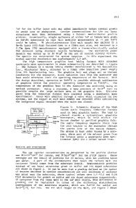
Abstract Herein, the Ni/SiO2/p-Si MIS diode was developed via the liquid phase epitaxy (LPE) process. The structural and surface morphology were investigated by XRD and SEM techniques. The electrical study of the device, Ni/SiO2/n-Si, demonstrates a worthy rectification and the electrical parameters of the Schottky diode have computed using the I-V characterization. Different dielectric parameters as capacitance (C), permittivity (ε’), dielectric loss (ε”), conductance and ac conductivity (σac) were evaluated. Moreover, their relation to bias dc voltage has been examined in the frequency range 10 Hz–20 MHz, temperature 303 K to 363 K and DC bias voltage from -2 V to 2 V. Also, the variable investigated parameters were found to be dependent upon temperature, frequency and bias voltage. Keywords MIS diode . Liquid phase epitaxial . X-ray diffraction . Series resistance . Diode ideality factor . Ac conductivity
1 Introduction Nowadays, metal-insulator/oxide-semiconductor (MIS/MOS) gaining importance in the current articles owing to its stable performance and modest fabrication process of metal/ semiconductor Schottky diodes and its important applications in integrated circuits and semiconductor devices, integrated circuits, solar cells sensors, magneto-resistance measurements, microwave mixers [1–5]. In the research articles of the photovoltaic, the metal/semiconductor Schottky diodes demonstrated different benefits like it has fast photoresponse, great signal to noise ratio and low forward resistance. Furthermore, the updated model of the metal/semiconductor Schottky diodes designed by depositing an interfacial layer between the metal layer and the
* I. M. El Radaf [email protected]; [email protected] 1
Solid State Electronics Laboratory, Solid State Physics Department, Physics Division, National Research Centre, Dokki, Giza 12622, Egypt
2
Microwave Physics and Dielectrics Department, National Research Centre, Dokki, Giza 12622, Egypt
3
Electron Microscope and Thin Films Department, Physics Division, National Research Centre, Dokki, Giza 12622, Egypt
4
Materials Physics and Energy Laboratory, College of Sciences and Art at ArRass - Qassim University, ArRass 51921, Saudi Arabia
semiconductor layer. The consistency of the native oxide layer of a few nanometer thicknesses at the metal/semiconductor Schottky diodes is unavoidable unless the devices are specially synthesized via the advanced methods [6]. The MOS and MIS contacts were formed via the deposition of the metal/ semiconductor contacts on an insulator or oxide layer which displayed better electrical properties than that of the metal/ semiconductor Schottky diodes [7–12]. The increasing barrier height in MIS photodetector occupied by an increase in the speed of the hot electrons which flow from semico
Data Loading...