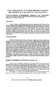
Defect and Raman Spectroscopy of Chemical Vapor Deposition Grown Diamond Films
- PDF / 688,068 Bytes
- 6 Pages / 390.24 x 621.9 pts Page_size
- 17 Downloads / 354 Views
concentration used during growth or ion implanting boron or carbon.", 2 It has been proposed that FE from diamond films is due to electron transport through defects, and films with higher sp2 and disordered structures have higher FE currents because they have more defects."' 2 Experimental studies have shown the existence of normally unoccupied surface states on the diamond (111) 2xl surface that have an energy 4.8 eV above the valence band3 , and defect states 2.0 and 4.1 eV below the conduction band of single crystal diamond.4 Theoretical studies of bulk diamond predict vacancy defects in an energy range 1-2 eV above the valence band.5 However, these states have an energy range that is too low to couple to states that can produce tunneling in FE.5 In this paper, we report photoelectron emission from CVD grown polycrystalline diamond films using visible light excitation at photon energies from 2.41 eV to 2.71 eV from an argon laser. The photoelectron emission rate is observed to have a quadratic dependence on the incident light power showing that the photoelectron emission process is a two-photon process involving electron emission from normally unoccupied states. The photoelectric yield increases rapidly as a function of incident photon energy. The photoelectric yield is observed to decrease as the methane to hydrogen gas concentration used during growth increases. EXPERIMENT Polycrystalline diamond films were grown using methane to hydrogen gas concentrations of 0.10%, 0.20%, 0.30%, 0.45%, 0.60% and 0.70%. The films were grown on polished 589 Mat. Res. Soc. Symp. Proc. Vol. 558 © 2000 Materials Research Society
conducting p-type Si (100) substrates using a hot-tungsten filament CVD reactor. Diamond nucleation was Experimental Set-up achieved using bias enhanced nucleation for 30 minutes. After this step, a thin Vacuum Chamber 10' Torr diamond film was deposited for 6 hours at a substrate temperature of 8700C and a pressure of 30 Torr. The It flow rate was 200 standard cubic centimeters per minute (sccm) and the methane flow rate was varied from 0.40 to 1.60 seem. The tungsten filament temperature was 22000 Microchannel plate C, The growth experiment was detector terminated by first shutting off the Argon laser methane flow while maintaining the sample, filament, and H- settings for 2 minutes. Then the filament, sample heater and H2 flow were turned off in Figure 1. Schematic of experimental set-up for that order. measuring the Kaman spectrum and photoelectron We perform photoelectron emission and Raman measurements emission. simultaneously on the same area of the sample. Our experimental setup is shown schematically in Fig. I The samples are studied in a vacuum chamber at a pressure • 10° Torr Light from a cw argon laser is directed via a microprism iand focussed on the sample to a spot having a diameter of 5-10 ýim. The Raman scattered light from the sample is collected by the focussing lens and focussed by a second lens on the entrance slit of a double monochromator. Photoelectrons enitted from the sample ar
Data Loading...