Defect Properties of Cathode Deposited Glow Discharge Amorphous Silicon Germanium Alloys
- PDF / 461,243 Bytes
- 6 Pages / 414.72 x 648 pts Page_size
- 114 Downloads / 400 Views
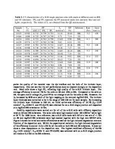
grown on c-Si to enable various junction capacitance and current measurements. These include capacitance vs. temperature and frequency (C-T-o)) [8], drive-level capacitance profiling [9] and sub-band-gap transient photocapacitance together with transient photocurrent [10]. RESULTS AND ANALYSIS We present the general optical and electrical properties of these films deposited at different flow rates of SiH4 in Table 1. The germanium content of each film was well determined by the electron microprobe method with an error less than lat.%. The optical gaps E0 4 and E 03 were obtained from optical absorption measurements on glass substrate samples. The dark ac conductivity activation energy, Ea, which we identify with the Fermi energy position, (Ea = EC - EF), was deduced from the C-T-co measurements for our Schottky diode samples. Table 1: Optical and electrical properties of cathode deposited glow discharge a-Sil-xGex:H alloys. E04 3 1 and E03 are the photon energies at which the absorption coefficient ccy4 = 104 cm- 1 and oC 03 = 10 c-n , respectively. Sample No. SiH 4 flow Ge Bandgap (eV) Ea (eV) Thickness (p.tm) (sccm) content E0 4 E 03 Optical C-T-wo 479
1.60
57.3 at.%
1.57
1.39
0.666
2.83
2.61
478 477 476 427
1.00 0.70 0.37 0.00
67.5 74.5 84.5 100
1.53 1.44 1.40 1.26
1.37 1.30 1.24 1.12
0.645 0.620 0.559 0.510
3.07 2.99 1.97
3.08 2.77 1.96 2.28
at.% at.% at.% at.%
-
Clearly, both the optical bandgap and the dark ac conductivity activation energy decrease monotonically with increasing Ge content. We also note that Ea is always less than one-half of E 04 (or even E0 3 ) implying that these alloys are effectively slightly n-type with a Fermi level above mid-gap. The fact that the film thicknesses obtained from capacitance match those derived from the optical absorption measurements indicates similar properties of films deposited on the different substrates. To determine the mid-gap defect densities in these high Ge content samples, we carried out drive-level capacitance profiling measurements at 100Hz for a series of temperatures between 290K and 350K. In Fig.l(a) we display typical drive-level capacitance profiling data for the sample with x = 0.57. It was observed that the drive-level density, NDL, does not exhibit any obvious temperature dependence in these samples. However, a clear temperature dependence of the drive-level density had indicated a well-defined defect band below the Fermi level in all USSC glow discharge a-Sil-xGex:H samples with lower Ge content (0.2 (x ( 0.5)[11]. For comparison, we plot the temperature dependent NDL data of one such sample with x = 0.5 in Fig.l(b). There are, we believe, two reasons that NDL might be temperature independent for the cathodic, larger Ge containing samples. The first is that the bulk Fermi level EFF may be too close to the quasi Fermi level, EF*, in deep depletion. In this case, we would be probing the entire deep depletion charge density at even the lowest measurement temperature so that NDL already has its maximum value. The second is that there
Data Loading...