Defects in Monocrystalline Silicon
The aggregation of instrinsic point defects (vacancies and Si interstitials) in monocrystalline silicon has a major impact on the functioning of electronic devices. While agglomeration of vacancies results in the formation of tiny holes (so-called “voids”
- PDF / 1,833,322 Bytes
- 20 Pages / 547.146 x 686 pts Page_size
- 15 Downloads / 475 Views
5. Defects in Monocrystalline Silicon
Defects in Mo
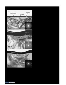
As the feature size continues to shrink in device industry, a thorough understanding of defect behavior in bulk silicon becomes more and more important. Three major defect types relevant to device performance have been identified: vacancy aggregates (known as “voids”, which usually have a size of less than 150 nm); Si interstitial clusters embedded in a network of dislocation loops, each of which extend over several microns (L-pits); and large grown-in oxygen precipitates. The latter generate stacking faults (OSF) during wafer oxidation. The voids form in the center of the crystal, while L-pits are observed in the outer region. The two concentric defect regions are usually separated by a small OSF ring. The type of defect that develops in the growing crystal is determined by a simple parameter: the ratio of
5.1
Technological Impact of Intrinsic Point Defects Aggregates ..... 102
5.2
Thermophysical Properties of Intrinsic Point Defects ...................... 103
5.3
Aggregates of Intrinsic Point Defects ..... 5.3.1 Experimental Observations ......... 5.3.2 Theoretical Model: Incorporation of Intrinsic Point Defects ............ 5.3.3 Theoretical Model: Aggregation of Intrinsic Point Defects ............ 5.3.4 Effect of Impurities on Intrinsic Point Defect Aggregation ............
5.4
104 104 107 109 112
Formation of OSF Ring.......................... 115
References .................................................. 117
to accurately simulate the aggregation process so that the defect behavior of semiconductor silicon can be precisely tailored to the needs of the device manufacturer. Additionally, the impact of various impurities on the aggregation process is elucidated.
the pull rate to the temperature gradient at the growth interface. In industry, crystals with only one type of defect – voids – are produced almost exclusively. The formation and behavior of voids has been studied intensively and is accurately described by current theoretical models. As the feature size is now approaching the void size, the growth of so-called “perfect silicon” with almost no detectable defects may be adopted. Furthermore, the doping of crystals with impurities like nitrogen or carbon is being widely investigated. These impurities can significantly reduce the defect size, but they may also have harmful effects, such as enhancing the generation of OSFs. Some models have recently been proposed which may allow us to predict some of the effects of impurities.
Part A 5
The aggregation of instrinsic point defects (vacancies and Si interstitials) in monocrystalline silicon has a major impact on the functioning of electronic devices. While agglomeration of vacancies results in the formation of tiny holes (so-called “voids”, around 100 nm in size, which have almost no stress field), the aggregation of Si interstitials exerts considerable stress on the Si matrix, which, beyond a critical size, generates a network of dislocation loops around the original defect. These dislocati
Data Loading...