Degradation of Luminescence from GaN During Electron Bombardment: Effects of Beam Voltage, Current and Scanned Area
- PDF / 259,421 Bytes
- 6 Pages / 612 x 792 pts (letter) Page_size
- 1 Downloads / 304 Views
DEGRADATION OF LUMINESCENCE FROM GaN DURING ELECTRON BOMBARDMENT: EFFECTS OF BEAM VOLTAGE, CURRENT AND SCANNED AREA E. M. Campo,* G. S. Cargill III,* J. Ramer,** M. Schurman,** and I. T. Ferguson** *Lehigh University, Bethlehem, PA 18015, [email protected] **EMCORE Corp., Somerset, NJ 08873
ABSTRACT Near-band-edge cathodoluminescence emission for some nominally undoped GaN samples decreases with time during electron bombardment in a scanning electron microscope. The rate of decrease depends on the incident beam voltage and current and on the size of the area being scanned, which is determined by the magnification used for the scanning electron microscope. Faster intensity decreases occur with lower beam voltages (10kV versus 20kV), higher beam currents (600nA or 200nA versus 35nA) and smaller scanned areas (120K magnification versus 15K magnification). For larger scanned areas, the maximum luminescence intensity occurs 10’s or 100’s of seconds after the start of electron bombardment, and the intensity then decreases with further bombardment. In some cases the size of the degraded region is larger than the bombarded area. These observations suggest that the degradation is caused by electromigration of impurities or other charged defects within the GaN resulting from local charging by electron bombardment.
INTRODUCTION It is well known that luminescence properties of GaN samples can be affected by electron beam irradiation. Some studies report complex changes in cathodoluminescence (CL) intensities and wavelengths caused by electron irradiation and attribute these changes to electromigration induced H and O redistributions [1]. Other studies report that electron irradiation strongly affects the CL properties of both n- and p-type GaN, increasing both near band-edge and lower energy luminescence, with these changes attributed to activating Mg acceptors and possibly creating deep levels, affecting uniformity of doping, creating vacancies and annealing out defects [2]. Chao et al. [3] reported on degradation of near band-edge luminescence, in some cases accompanied by growth of deep-level emission and in other cases accompanied by degradation of deep-level emission, for MBE, MOCVD and HVPE grown GaN films. In an earlier paper [4], we reported degradation dependence on beam current and magnification for 20 kV beam voltage for undoped MOCVD GaN samples. In the present paper we extend these measurements to 10 kV beam voltage and to other, similar samples.
EXPERIMENTAL
G6.27.1
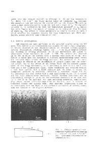
Lateral epitaxial overgrowth (LEO) GaN samples were grown on sapphire substrates using SiNx masks by MOCVD using an EMCORE SpectraBlue 6x2 reactor specifically developed for growth of optoelectronic devices. The growth temperature was 1000°C and the growth rate was 1.6µm/hr. A 2 µm thick GaN buffer layer was first grown on the sapphire substrate, followed by a 100nm thick SiNx mask layer in which patterns of windows of different widths and periods were produced by lithographic methods. The data shown in this paper are for a window-mask repetition p
Data Loading...