Deposition and characterization of nanostructured Cu 2 O thin-film for potential photovoltaic applications
- PDF / 453,510 Bytes
- 7 Pages / 584.957 x 782.986 pts Page_size
- 102 Downloads / 359 Views
Fan Wu and Jagdish Narayanb) Department of Materials Science and Engineering, North Carolina State University, Raleigh, North Carolina 27695-7907
Colin McMillen Department of Chemistry, Clemson University, Clemson, South Carolina 29634
Githin F. Alapatt and Kelvin F. Poole Holcombe Department of Electrical and Computer Engineering, Clemson University, Clemson, South Carolina 29634
Shiou-Jyh Hwu and Dino Sulejmanovic Department of Chemistry, Clemson University, Clemson, South Carolina 29634
Matthew Young, Glenn Teeter, and Harin S. Ullal National Renewable Energy Laboratory, Golden, Colorado 80401 (Received 20 November 2012; accepted 8 May 2013)
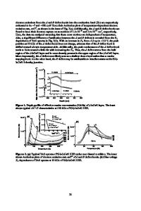
Copper (I) oxide (Cu2O) is a direct band gap semiconductor with p-type conductivity and is a potential candidate for multi-junction solar cells. In this work, incoherent light source based photoassisted metal-organic chemical vapor deposition (MOCVD) was used to deposit high quality Cu2O thin films on n-type ,100. silicon and quartz substrates. X-ray diffraction studies reveal that crystalline Cu2O is deposited. UV-Vis-NIR spectroscopy results indicated a band gap of 2.44 eV for Cu2O thin films. Transmission electron spectroscopy results show that the Cu2O film grows in the form of three-dimensional islands composed of smaller nanocrystalline grains in the range of 10–20 nm. I–V measurements indicate that the Cu2O/n-Si device fabricated using the MOCVD process has a lower dark current density than other devices reported in the literature. I. INTRODUCTION
The cost of photovoltaic (PV) modules in the last five decades has decreased exponentially. The growth rate of the global PV market was about 70% per year from 2007 to 2011.1 As early as 1980, an economic analysis suggested that Si is the best material for terrestrial PV applications.2 This prediction still holds true, because 90% of the currently manufactured solar cells are based on bulk Si. Highest demonstrated AM1.5G efficiency of a passivated emitter with rear locally diffused (PERL) crystalline silicon solar cells is 25%.3 Using commercial-grade p-type silicon wafers, recent work of Wang et al.4 has led to the development of a commercial version of the PERL cell with a record production-level AM1.5G efficiency of 20.3%. Further improvements in the efficiency of silicon-based a)
Address all correspondence to this author. e-mail: [email protected] b) This author was an editor of this focus issue during the review and decision stage. For the JMR policy on review and publication of manuscripts authored by editors, please refer to http://www.mrs. org/jmr-editor-manuscripts/ DOI: 10.1557/jmr.2013.150 J. Mater. Res., 2013
solar cells can be achieved by the use of multi-terminal multi-junction solar cells.5 For the new materials, the cost of the raw materials and their atomic concentration in the earth’s crust can give a good indication of the relative cost of that material in a large-scale application. For generating PV electricity at a lower cost ($/kWh) than conventional energy sources, the following criteria must be used
Data Loading...