Deposition and Electrical Characterization of Dielectric/Ferromagnetic Heterostructure
- PDF / 613,389 Bytes
- 8 Pages / 415.8 x 637.2 pts Page_size
- 66 Downloads / 366 Views
363 Mat. Res. Soc. Symp. Proc. Vol. 602 @ 2000 Materials Research Society
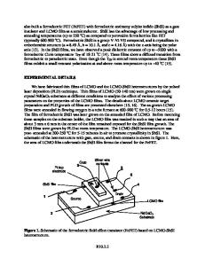
(a)
Drain
Source Pt
,
•
:a
P
...
ZT
B
(b)
1. (a) The device configuration; (b) Cross section TEM picture of the device.
364
[8]. Both the 150 rum layer of PZT and 50 rim layer of LCMO are grown by pulsed laser deposition technique using a KrF excimer laser (X,=248 nm). A (100)-orientated single crystal of STO doped with I at. % of Nb is treated with diluted HF solution to achieve atomic flat surface [9] and served both as substrate for film growth and as gate for the device. Growth conditions including the heater temperature and the oxygen pressure are optimized to achieve good film quality for both layer and epitaxial interfaces between them. XRD patterns show (001) orientation for both layers. After the film deposition, a device structure is then defined using standard photolithography and chemical etching. Fig. 1(b) is the TEM picture of our device showing the smooth interfaces, which are crucial for reproducible device performance. Resistivity of the LCMO channel is obtained by standard four probe technique with temperature from 4K to 300K after pulsing the gate with positive and negative 6 volts. Experiments are performed both with and without a magnetic field of 6T. RESULTS Fig. 2 shows the temperature dependence of resistivity of the LCMO channel measured before and after pulsing the gate with positive and negative 6 Volts, which, basically, induce additional electrons and holes in the channel, respectively. The ER, defined as (R(E)-R(0))/R(0) is about 76% at Tp after negative 6V pulsing. The negative pulse produces much larger effect than the positive one, reflecting the hole conducting nature of the CMR channel. In Fig. 3 we present data on the combined consequences of the electrical and magnetic fields for the transport in the CMR channel. We can reduce the channel resistance by using either -6V volts pulsing (from A to B) or 6T magnetic field (from A to C). Most interestingly, both B and C can be further changed into D if both electrical pulse and magnetic fields are used. In Fig. 4, we show the ER and MR data separately. It is noteworthy that not only their sizes are comparable, but also they are complimentary with each other. There is an expected temperature shift in the MR data, caused by the spin aligning effect of magnetic field. But the ER peak temperature remains the same. Our device shows reasonable large ER effect even at room temperature. In Fig.5 we show a series of I-V curves of the CMR channel after gate pulsing of -2, -4, -6 Volts respectively. Obviously, this large modulation of channel resistance cannot be cause by carrier density modulation only, which is less than 0.25%. Our experimental data strongly suggests that the induced holes are not doped homogeneously, indicating the electronic inhomogeity of the manganite channel. According to the phase reparation picture, in the CMR manganites the FM (metallic) and the charge ordered (CO) states coexist in a broad range of phase space [3]. The size and t
Data Loading...