Deposition Of BaTiO 3 Thin Films And MgO Buffer Layers On Patterned GaAs Substrates For Integrated Optics Applications
- PDF / 548,142 Bytes
- 6 Pages / 612 x 792 pts (letter) Page_size
- 71 Downloads / 361 Views
C11.23.1
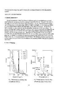
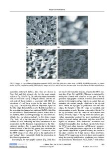
Deposition Of BaTiO3 Thin Films And MgO Buffer Layers On Patterned GaAs Substrates For Integrated Optics Applications Ding-Yuan Chen, Timothy E. Murphy, and Jamie D. Phillips Department of Electrical Engineering and Computer Science The University of Michigan, Ann Arbor, MI 48109, U.S.A. Email:[email protected] ABSTRACT This work addresses the need for thick layers of ferroelectric thin films on semiconductors for integrated optics applications. The deposition of BaTiO3 thin films with MgO buffers on patterned GaAs substrates is presented as an approach to achieve crack-free optical waveguiding structures. Cracking and peeling of the thin films are observed on patterns with lateral dimensions exceeding 60 microns and nearly crack-free thin films for patterns with lateral dimensions of a few microns. The cracking and peeling of the thin films is attributed to thermal expansion mismatch during the heating and cooling steps of the deposition process. A thin film stress and fracture model is used to analyze the phenomenon. Reduced cracking and peeling on the patterned features are attributed to strain relief on the patterned features. The inclusion of thick AlxOy buffer layers obtained through wet-oxidation of AlGaAs prior to BaTiO3/MgO deposition are presented as a means of obtaining electro-optic waveguide structures on GaAs. INTRODUCTION The integration of ferroelectric thin films with semiconductors is of high interest for integrated optics and optoelectronic integrated circuits (OEIC). Ferroelectric oxides such as BaTiO3 are transparent in the visible and infrared [1] and possess strong electro-optic coefficients making them attractive for active and passive optical components. The development of optical waveguide devices based on ferroelectric/semiconductor integration is hampered by several wave-guiding and structural requirements: 1. a highly-oriented ferroelectric film is needed to obtain large electro-optic response. 2. a chemically stable buffer to prevent interdiffusion 3. sufficiently thick crack-free films 4. the achievement of low-loss ridge waveguides through etching or other techniques [2], and 5. the achievement of the proper refractive index contrast for waveguiding and to prevent leakage to the substrate. The integration of ferroelectrics on compound semiconductors such as GaAs is attractive due to the ability to integrate optoelectronic sources and detectors. Structures consisting of BaTiO3/MgO/GaAs show potential for integrated optics, where MgO facilitates cube-on-cube epitaxy of the materials, prevents arsenic and oxygen interdiffusion at deposition temperatures, and provides a low refractive index for optical confinement [3]. Parameters of these materials in the bulk form are given in Table 1. Highly oriented BaTiO3 thin films on GaAs have been previously demonstrated using MgO buffer layers [4]. The BaTiO3/MgO/GaAs structures have been problematic for integrated optics applications due to the inability to obtain sufficiently thick MgO cladding layers for optical waveguiding and the p
Data Loading...