Determination of indenter tip geometry and indentation contact area for depth-sensing indentation experiments
- PDF / 224,148 Bytes
- 7 Pages / 612 x 792 pts (letter) Page_size
- 80 Downloads / 545 Views
MATERIALS RESEARCH
Welcome
Comments
Help
Determination of indenter tip geometry and indentation contact area for depth-sensing indentation experiments K. W. McElhaney, J. J. Vlassak, and W. D. Nix Department of Materials Science and Engineering, Stanford University, Stanford, California 94305 (Received 26 September 1996; accepted 31 October 1997)
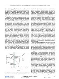
The phenomena of pile-up and sink-in associated with nanoindentation have been found to have large effects on the measurements of the indentation modulus and hardness of copper. Pile-up (or sink-in) leads to contact areas that are greater than (or less than) the cross-sectional area of the indenter at a given depth. These effects lead to errors in the absolute measurement of mechanical properties by nanoindentation. To account for these effects, a new method of indenter tip shape calibration has been developed; it is based on measurements of contact compliance as well as direct SEM observations and measurements of the areas of large indentations. Application of this calibration technique to strain-hardened (pile-up) and annealed (sink-in) copper leads to a unique tip shape calibration for the diamond indenter itself, as well as to a material parameter, a, which characterizes the extent of pile-up or sink-in. Thus the shape of the indenter tip and nature of the material response are separated in this calibration method. Using this approach, it is possible to make accurate absolute measurements of hardness and indentation modulus by nanoindentation. I. INTRODUCTION
Indentation experiments have led to well-established methods for determining the mechanical properties of materials in small volumes.1–9 The availability of depthsensing indentation instruments with capabilities for measuring displacements on the order of nanometers now makes it possible to study mechanical properties of thin films and other finely structured materials where small volumes need to be probed.1,4 Research on nanoindentation has shown that elastic moduli,2,4,7,10 hardness,1,35 and time-dependent deformation effects11 can be measured, provided the area of contact between the indenter and the test material is known. Indeed, determining the contact area from the indentation forces and displacements is central to the study of mechanical properties of materials in small volumes by nanoindentation. It is widely known that the contact area at a particular depth of indentation depends not only on the shape of the indenter (diamond) but also on the elasticplastic response of the material being indented. In some cases the volume of material displaced by the indentation pushes out to the sides of the indenter and forms a pile-up of material, making the projected contact area larger than the cross-sectional area of the indenter at that depth. For other materials, the displaced volume is accommodated mainly by far-field elastic displacements, producing what is called a sink-in effect. In this case the contact area is less than the cross-sectional area of the indenter at that depth. Although the pile-up and s
Data Loading...