Development of Si Microliquid Processing using Piezo Actuator
- PDF / 367,465 Bytes
- 6 Pages / 432 x 648 pts Page_size
- 67 Downloads / 314 Views
Development of Si Microliquid Processing using Piezo Actuator
Muneki Akazawa, Shunki Koyanagi and Seiichiro Higashi Department of Semiconductor Electronics and Integration Science, Graduate School of Advanced Sciences of Matter, Hiroshima University, Kagamiyama 1-3-1, Higashi-Hiroshima, 739-8530, Japan
ABSTRACT The tip of a Si rod was melted by laser diode (LD) irradiation and we succeeded in dropping small Si droplets by vibration of the Si rod using a piezo actuator. We confirmed multiple small Si droplets under a condition of the resonance frequency of 5.8 kHz for the rod length of 6.0 mm. We observed ejection of droplets from a cone edge of molten Si and the minimum width of the solidified Si was ~ 1 Pm in diameter. The solidified Si show high crystallinity with the Raman scattering TO phonon band of 515.6 cm-1. INTRODUCTION The formation of highly-crystallized Si films at a low temperature has attracted much attention because of their potential advantages in the application to active and contact layers of thin film transistors (TFTs) and solar cells [1]. In that regard, many studies based on plasma enhanced chemical vapor deposition (PECVD) techniques have so far been made to enhance the growth rate and to improve the film quality, especially the crystallinity [2,3]. Recently, we have proposed a new rapid crystallization technique using a molten Si droplet ejected from a boron nitride cylinder with a 100 μmφ nozzle heated at 1850 K [4]. By dropping multiple small droplets like ink-jet printing, this technique has the possibility to form high crystallinity Si films without severe heat damage to the substrate [5,6]. In our previous work, we have found that pseudo-epitaxial growth occurs by dropping Si microliquids on hydrogen(H)-terminated Si wafer surfaces[6]. It is quite interesting that solidified Si droplets are easily removed from H-terminated Si wafer, however, they show (100) and (110) orientations when dropped on H-terminated (100) and (110) surfaces, respectively. Therefore, if we could deposit multiple small droplets on H-terminated wafer, we can fabricate orientation-controlled Si thin films by this method. However, there are two critical issues. One is the Boron contamination from the cylinder wall, and the other one is large droplet size (~ 300 Pm).
407
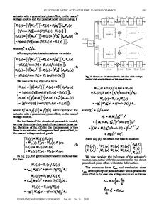
Fig. 1 Schematic diagram of Si microliquid processing equipments using a piezo actuator.
Fig. 2 Snapshots of a Si microliquid ejecting from the tip of the rod.
In this work, the tip of a single crystalline Si rod was melted by laser diode (LD) irradiation and we attempted to drop smaller pure Si liquid by vibration of the Si rod using a piezo actuator. EXPERIMENT The experimental setup is shown in Fig. 1. A 525 Pm-thick n-type Si(100) wafer was cut into 6 ~ 20 mm long rods with the width of 520 Pm. The Si rod was connected to a piezo actuator. The distance between the tip of the Si rod and a quartz substrate was set at 1 mm. A laser diode (LD) light, with a wavelength of 807 nm and a power of ~ 15 W was irradiated to the tip of the Si rod to fo
Data Loading...