Direct Growth of Single Walled Carbon Nanotubes for the Characterization of Structural and Electronic Properties
- PDF / 3,909,624 Bytes
- 6 Pages / 612 x 792 pts (letter) Page_size
- 84 Downloads / 333 Views
1081-P04-02
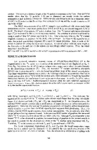
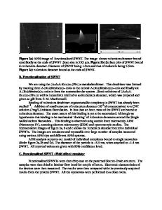
Direct Growth of Single Walled Carbon Nanotubes for the Characterization of Structural and Electronic Properties Jianfeng Wu, Joel Walenza-Slabe, Timothy Gutu, and Jun Jiao Department of Physics, Portland State University, P.O. Box 751, Portland, OR, 97207-0751 ABSTRACT Fabricating horizontally aligned single wall carbon nanotubes (CNTs) with controlled properties has been one of the significant challenges for field-effect transistor (FET) applications. This report demonstrates a novel procedure for the fabrication of horizontally aligned single walled CNTs using the focused ion beam (FIB) and chemical vapor deposition (CVD). This method allows the morphologies, internal structures, and elemental compositions of CNTs to be directly analyzed in the scanning electron microscope (SEM) and transmission electron microscope (TEM) and avoids any sample preparation procedures that might alter the structure of the CNTs. The techniques of electron beam and ion beam induced deposition (EBID and IBID) of Pt electrodes to the CNT ends were compared and both were found to produce metal contamination around the target area. The fabrication of large area electrodes to assist in testing the CNT’s electronic properties, including contact resistance and I-V characteristics was investigated. Using this fabrication technique we were able to perform an I-V sweep on a CNT circuit as well as detect the metal contamination on the CNTs which occurred as a result of electrode deposition. INTRODUCTION Since the demonstration of the CNT FET in 1998, intensive efforts have been made to fabricate CNT-based devices and to characterize their electronic properties [1]. CNTs have unique ballistic transport characteristics and high carrier mobility which have attracted a great deal of attention [2-3]. However, the techniques used to grow single CNTs usually result in wide variations of the shape, size and internal structure on which their electronic properties are based. It is this variation that necessitates a methodology to connect those electronic properties to their observed structure. The TEM can provide the most direct information on the internal structure of single wall CNTs. However, TEM sample preparation requires suspending the CNTs in solvent followed by their random deposition onto a TEM grid. In preparation for the electronics test CNTs are subject to random selection. First, they are sonicated to release them from the growth substrate. Next, they are dispersed throughout a dielectric medium and aligned across polarized, predefined electrodes [4]. In another method, single walled CNTs are grown directly on catalyst patterned on the wafer and further lithographic steps are employed to deposit lead contacts on the ends of individual CNTs [5]. Using these methods, one unique nanotube circuit can either be observed in the TEM or electronically probed but it cannot be analyzed for both of these properties. The ideal experiment would combine these procedures on a specially designed TEM grid. This report demonstrates a novel procedu
Data Loading...