Direct Observation by Transmission Electron Microscopy of the Early Stages of Growth of Superconducting Thin Films
- PDF / 2,158,711 Bytes
- 4 Pages / 420.48 x 639 pts Page_size
- 28 Downloads / 390 Views
DIRECT OBSERVATION BY TRANSMISSION ELECTRON MICROSCOPY OF THE EARLY STAGES OF GROWTH OF SUPERCONDUCTING THIN FILMS M. GRANT NORTON, LISA A. TIETZ, SCOTT R. SUMMERFELT and C. BARRY
CARTER, Department of Materials Science and Engineering, Cornell University, Ithaca, NY 14853.
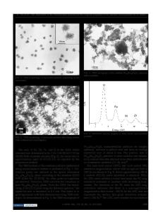
ABSTRACT The fabrication of high quality thin films often depends on the early stages of the growth process during which epitaxy is established. The substrate surface structure generally plays a critical role at this stage. Many observations of the high-Tc superconductor film-substrate interface structure and chemistry have been made by transmission electron microscopy (TEM) of cross-section samples. Ion-milling induced damage, however, can be severe in these specimens. In the present study, the early stages of the growth of high Tc superconducting thin films of YBa2Cu3O7-S have been studied by TEM using a technique which requires no post-deposition specimen preparation. INTRODUCTION Many techniques have been used to deposit thin films of the superconducting oxide YBa2Cu3O 7.8 (YBCO). Deposition by pulsed laser ablation from stoichiometric bulk samples has received a lot of attention because it enables high quality superconducting films to be formed 'in-situ' [1]. Determination of film properties and microstructure of laser deposited films have been reported [2,3] and also analysis of the mechanism of the ablation process by examination of plume constituents [4]. The nucleation and growth of YBCO thin films has however received little attention [5]. The formation of high quality films depends on the grain structure and orientation of the deposited material and this will be determined during the early stages of film growth. In this study transmission electron microscopy (TEM) is used to observe the initial stages of film growth. Damage is often introduced during preparation of YBCO thin film samples for TEM analysis [6]. This damage can be avoided by depositing films directly onto clean, wellcharacterized, electron transparent substrates. This technique enables film nucleation and growth to be studied directly using TEM. The final film microstructure may be different from the initial film microstructure but it is these early stages which will control the final microstructure and hence properties. EXPERIMENTAL The substrate material used was single-crystal (001)-oriented MgO. The samples were prepared from bulk material for examination in the TEM in the usual manner. After ion-milling the thin-foils were chemically cleaned to remove sputtered metallic deposits, then annealed at 1350°C in air for 10 minutes. Care was taken to avoid any possible contamination from the furnace. Ultra thin films of YBCO were deposited onto a thin foil substrate prepared as above. The films were formed by pulsed laser ablation from a stoichiometric bulk pellet. The experimental technique for film formation is described elsewhere [7]. Briefly, a KrF excimer laser was focussed onto a rotating target of YBCO. The thin-foil substrate was held 5 cm away on a heated stage.
Data Loading...


