Directed Growth of Branched Nanowire Structures
- PDF / 481,767 Bytes
- 7 Pages / 612 x 801 pts Page_size
- 49 Downloads / 272 Views
Branched Nanowire Structures
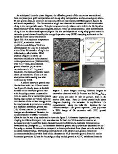
Kimberly A. Dick, Knut Deppert, Lisa S. Karlsson, Magnus W. Larsson, Werner Seifert, L. Reine Wallenberg, and Lars Samuelson Abstract We describe the production of hierarchical branched nanowire structures by the sequential seeding of multiple wire generations with metal nanoparticles. Such complex structures represent the next step in the study of functional nanowires, as they increase the potential functionality of nanostructures produced in a self-assembled way. It is possible, for example, to fabricate a variety of active heterostructure segments with different compositions and diameters within a single connected structure. The focus of this work is on epitaxial III–V semiconductor branched nanowire structures, with the two materials GaP and InAs used as typical examples of branched structures with cubic (zinc blende) and hexagonal (wurtzite) crystal structures. The general morphology of these structures will be described, as well as the relationship between morphology and crystal structure.
Introduction There has recently been much interest in the production of branched dendritic nanowire structures. The higher degree of complexity in such structures increases the potential for nanowire applications by increasing the number of connection points and providing a means for parallel connectivity and interconnection of functional elements. In addition, such structures facilitate studies of certain growth parameters, such as nucleation, that are difficult to study in single wires. Many types of structures have been produced by a variety of techniques. Self-assembled solution-based techniques have been used to produce branched CdSe,1,2 PdSe,3 CdS,4 MnS,5 CdTe,6 and PdMO4.7 Similarly, selfassembled branched structures can be produced by physical vapor deposition (PVD) or chemical vapor deposition (CVD). An enormous variety of structures have been synthesized using ZnO8–12 on a variety of nanowire base materials, but SiOx13 and WO complex structures14 have also been reported. The inclusion of an impurity material, such as Sn, often allows for particle-assisted CVD of materials, including ZnO,15,16 SnO,17 SiO2 and Si,18
MgO,19 In2O3,20 and CdS.21 Pre-formed nanoparticles can also be added to already grown nanowires to form hierarchical branched structures, as has been demonstrated for GaP,22–24 InP,24 GaAs,24 InAs,24–26 AlN, and GaN27 using metalorganic vapor-phase epitaxy (MOVPE); for InN and GaN28 using CVD; for Si29 using laser ablation; and for GaAs30 using molecular-beam epitaxy (MBE). Further, branched structures formed by the merging of two particle-assisted BN nanowires have been demonstrated.31 Hierarchical branched structures may be seen as the natural next step in nanowire studies, as they offer the scaling advantages of nanowires in more complex, multifunctional form. For example, it is well known that the properties of nanowires can be tuned by varying such factors as diameter and composition; compositional changes in particular can be exploited in the form of heterostructure
Data Loading...


