Domain Structure of Thick GaN Layers Grown by Hydride Vapor Phase Epitaxy
- PDF / 1,867,911 Bytes
- 6 Pages / 417.6 x 639 pts Page_size
- 15 Downloads / 326 Views
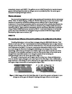
Cite this article as: MRS Internet J. Nitride Semicond. Res. 4S1, G3.16(1999) ABSTRACT The crystal structure and surface morphology of hydride vapour phase epitaxy grown thick (12-105 pim) GaN layers have been investigated as a function of growth rate using several structure sensitive techniques like atomic force microscopy (AFM), x-ray diffraction (XRD) in o-20 and 0)-rocking curve measurements as well as low temperature photoluminescence (PL). PL and XRD measurements reveal rather narrow lines: full width at half maximum (FWHM) values of the strongest donor-bound exciton line are in the range from 6.0 to1.8 meV and o0-20 FWHM values are between 80 and 23 arcsec indicating good structural quality of the films. The o)-rocking curves show a single peak for the thinnest films with a FWIM of 250 arcsec and multiple peaks with FWHIM of about 250-350 arcsec in thicker films indicating the formation of several high-quality domains when increasing either thickness or growth rate. Optical microscopy and AFM images reveal a domain type of morphology and also show an appearance of spiral hillocks in layers grown at growth rates exceeding a critical value. We interpret these results as dominating 2D multilayer growth at low growth rates, and competing 2D multilayer and spiral growth mechanisms at high growth rates. INTRODUCTION The growth of GaN is challenging, in part due to the independent optimisation of many growth parameters, and also due to the constraint of heteroepitaxy. Typically, sapphire or SiC substrates are used for substrates, although they are not lattice matched to the GaN layers. Thick hydride vapour phase epitaxial (HVPE) GaN layers on sapphire offer great potential as an alternative substrate for subsequent nitride growth. Studies by other researchers suggest that the application of thick GaN films for homoepitaxial growth of MOVPE GaN films may lead to improved optical and crystalline characteristics of the material [1,2]. From this point of view, it is very important to reach higher growth rates in HVPE growth while maintaining acceptable quality of the material. It has been found by other authors that the properties of thin GaN layers (several l.tm) are very different from those of thicker layers (over 20 l.tm), but while the thin MOVPE grown GaN layers have been intensively studied recently, there are a limited number of reports focused on thick films [2-5]. The growth mechanism of HVPE grown GaN is not fully understood at present, also its influence on the material properties is still far from complete. In this study, we have examined the optical and structural properties as well as the morphology of the HVPE GaN layers as a function of growth rate in order to gain insight into the growth mechanism and its relationship to the structural characteristics.
G 3.16 Mat. Res. Soc. Symp. Proc. Vol. 537 © 1999 Materials Research Society
EXPERIMENTAL All samples used in this study were grown under atmospheric pressure in a horizontal HVPE system. The sources for the V and III elements were NH 3 and metal Ga,
Data Loading...