Drastic Reduction of Threading Dislocation Density of AlGaN on SiC Wafer by Using Highly-Si-Incorporated AlGaN Superlatt
- PDF / 132,440 Bytes
- 6 Pages / 595 x 842 pts (A4) Page_size
- 77 Downloads / 376 Views
Drastic Reduction of Threading Dislocation Density of AlGaN on SiC Wafer by Using Highly-Si-Incorporated AlGaN Superlattice
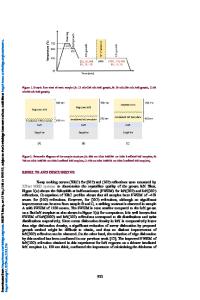
Hideki Hirayama1, Makoto Ainoya1,2, Atsuhiro Kinoshita12, Akira Hirata2 and Yoshinobu Aoyagi1 1 The Institute of Physical and Chemical Research (RIKEN), 2-1, Hirosawa, Wako-shi, Saitama, 351-0198, Japan, [email protected] 2 Department of Chemical Engineering, Waseda University, 3-4-1, Okubo, Shinjuku-ku, Tokyo, 169-8555, Japan ABSTRACT A new in-situ technique to reduce threading dislocation density (TDD) within submicron growth is demonstrated by using metal-organic vapor-phase epitaxy (MOVPE). We achieved drastic reduction of TDD of AlGaN buffer on SiC substrate by inserting highly-Siincorporated AlGaN/ undoped AlGaN superlattice (SL). TDD of AlGaN was decreased from 2×10¹⁰ to 7×107 cm-2 by inserting the SL with the total growth thickness of 0.8 µm. Si incorporation in AlGaN SL was estimated to be 1.2×1020 cm-3. This technique is exactly insitu process without complicated fabrication processes, and the surface is kept flat throughout the total growth. This method is especially useful on SiC wafer in order to prevent cracks with thin growth layer. We confirmed the similar effects for GaN and AlGaN buffer on sapphire substrates.
INTRODUCTION GaN and related compound semiconductors are one of the most attractive materials for blue, violet and ultraviolet (UV) light emitting diodes (LEDs) and laser diodes (LDs), or high speed, high power transistors. GaN or AlGaN buffers on SiC or sapphire substrates contains high-density (109-1011 cm-2) threading dislocations (TDs) grown with usual bulk growth technique. The dislocation density significantly influences the device performances such as efficiency or lifetime of LDs, photo diodes or transistors, because it becomes the origin of non-radiative recombination centers or carrier leak passes. So, the reduction of threading dislocation density (TDD) is one of the most important subject both for electrical and optical devices. We have been working on 300nm-band UV emitting devices using (Al)GaN/AlGaN or InAlGaN/InAlGaN quantum wells (QWs) [1]. For UV device applications, wide bandgap AlGaN buffer with low TDD is necessary, especially when using GaN/AlGaN QW systems. Several techniques have been reported for the reduction of TDDs such as LT-GaN [2], ELO [3,4], Pendeo-Epitaxy [5,6], FIELO [7] or anti-surfactant mediated buffer [8]. It is remarkable that low dislocation density of 105-106 cm-2 is possible using ELO, PendeoEpitaxy or FIELO technique. However, these methods need complicated fabrication G1.3.1
processes and rigid growth mode control. Also thick overgrown layer (several microns) is necessary to obtain flat surface. It was already reported that the TDD was reduced by Si doping into GaN layer [9]. However, the reduction ratio was not so high, because high density Si doping in GaN was impossible in order to prevent clacks on the surface. In this paper, we propose a new in-situ technique to reduce TDD by using GaN related superlattice (
Data Loading...