Dual-Gate SiO 2 /P3HT/SiN x OTFT
- PDF / 149,981 Bytes
- 6 Pages / 612 x 792 pts (letter) Page_size
- 15 Downloads / 312 Views
I9.3.1
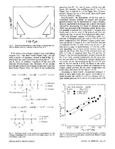
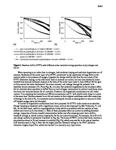
Dual-Gate SiO2/P3HT/SiNx OTFT Flora Li, Sarswati Koul, Yuri Vygranenko, Peyman Servati, and Arokia Nathan Department of Electrical and Computer Engineering, University of Waterloo, Waterloo, Ontario, Canada N2L 3G1 ABSTRACT This paper reports on a new organic thin-film transistor (OTFT) based on a dual-gate configuration. This dual-gate OTFT is useful in circuit applications from the standpoint of providing control over selected device parameters for enhanced circuit reliability. Moreover, the dual-gate structure can shield parasitic effects in vertically integrated electronics, making it particularly promising for active matrix display and imaging applications. The dual-gate OTFT also lends itself as a highly functional test structure for characterization of interface integrity of the active organic and dielectric layers. In this work, the dual-gate OTFT is fabricated using regioregular poly(3-hexylthiophene) (P3HT) as the organic semiconductor layer. The bottomgate employs silicon dioxide (SiO2) as the gate dielectric, whereas the top-gate employs a lowtemperature amorphous silicon nitride (SiNx) as the passivation dielectric. The voltage on the bottom-gate has a distinct influence on the threshold voltage, subthreshold slope, on-current, and leakage current of the top-gate TFT. Similar dependence of the bottom-gate TFT characteristics on the top-gate voltage is observed. This design provides a means of characterizing the density of states of the bottom P3HT/SiO2 and top P3HT/SiNx interfaces, and conveys insight into the underlying transport mechanisms. The ability to control selected TFT parameters (e.g., threshold voltage) using the dual-gate OTFT structure is attractive for circuit integration applications in active matrix displays and imagers. INTRODUCTION Research in organic thin-film transistors (OTFTs) over the last ten years has made significant progress, as improvements are seen in both device performance and innovative fabrication technologies [1-3]. These accomplishments, coupled with the film flexibility and various processability advantages offered by organic materials, have opened up numerous opportunities for organic electronics in areas in which low-temperature processing, large area coverage, mechanical flexibility, and overall low cost are required. Applications envisioned for OTFTs include active matrix organic light-emitting diode (AMOLED) displays, large-area flexible displays, electronic paper (e-paper), low-cost and low-end printable electronic devices such as radio-frequency identification (RFID) tags and smart cards, and sensor arrays [4,5]. One of the promising applications of OTFTs is its use as an on-pixel switching element in active matrix displays, similar to the functions that are currently fulfilled by amorphous silicon (a-Si) TFTs in liquid crystal displays [6], OLED displays [7], and imaging applications [8]. Active matrix backplane electronics based on OTFTs are particularly attractive for a new generation of flexible, lightweight displays and electronic paper [5,9]. Deve
Data Loading...